OPTi-based 386/486 Hybrid Motherboard - Part 2
In part 1 I did a walkthrough of the main components on this interesting 386/486 hybrid motherboard from 1993.
In part 2, let's explore some ways we can get more from it. Here is my shortlist to try out:
1) Add more memory.
2)
Max out the size of the L2 cache.
3) Add a math coprocessor.
4) Install a Cx486DLC CPU.
5) Install an 80486
CPU.
6) Add a VLB graphics card and multi I/O card.
Expansion Options
Adding more Main Memory
The motherboard came with 4 MB of 70 nanosecond SIMMs in bank 0. I dug out a further 4 MB, also 70 ns and installed them in bank 1. Some boards don't like mixing memory of differing speeds, even in different banks. This won't give much, if any, performance gains, but does mean we can run more demanding games up to around 1994 if coupled with a CPU upgrade. All benchmark tests were done with this 8 MB installed:
L2 Cache Increase from 128 KB to 256 KB
The motherboard came with 128 KB of 20ns level 2 cache installed. Not bad for any 386, but it's not the fastest and the board can support twice that. I ran some throughput tests using CacheChk version 7 and SpeedSys v4.78. Afterwards I installed a further 128 KB (15ns) in the second bank and re-ran the same tests.
Cache page for more information on cache sizes and how to calculate the best amount for your board.
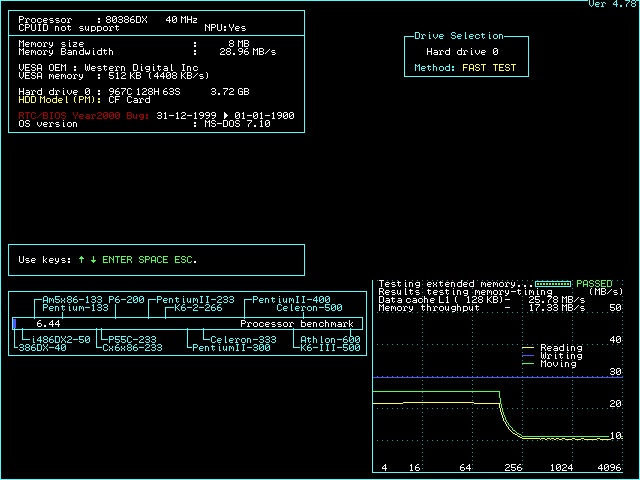
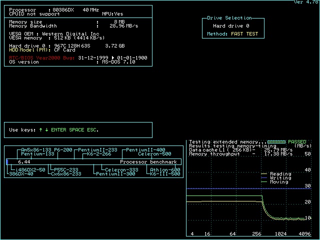
Am386DX-40, SpeedSys v4.78 with 128 KB L2 cache (left), and 256 KB L2 cache (right)
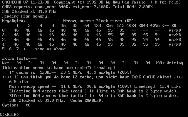
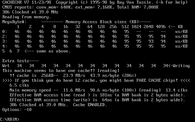
Am386DX-40, CacheChk 7 with 128 KB L2 cache (left), and 256 KB L2 cache (right)
These L2 throughput results of around 23.9 MB/s for both 128KB and 256KB sizes indicate that bank interleaving is *not* being used when I use both banks - I would have expected interleaving to work with both banks populated. It could be that interleaving is only enabled when the board runs in 486 mode - one Vogons member said interleaving only kicks in on burst reads, so 486 only - though the chipset datasheet just says "Two cache banks are required to interleave and realize the performance advantages of this cache scheme. Cache sizes of 128KB and 512KB are single bank caches, while 64KB and 256KB cache sizes are double bank.". It is also entirely possible that the chipset only enables bank interleaving when you have sufficient main memory to really 'need' it, or it is disabled in the BIOS and my MR BIOS doesn't have the option to enable/disable it - if you have an AMI BIOS let me know if cache bank interleaving is a visible selection.

Cache bank 1 and its Tag now populated with 15ns SRAMs
I also re-ran these tests after I set the motherboard jumpers to underclock the CPU to 33 MHz, as I want to be able to test the effectiveness of different cache sizes in conjunction with different CPUs later, two of which run at 33 MHz.
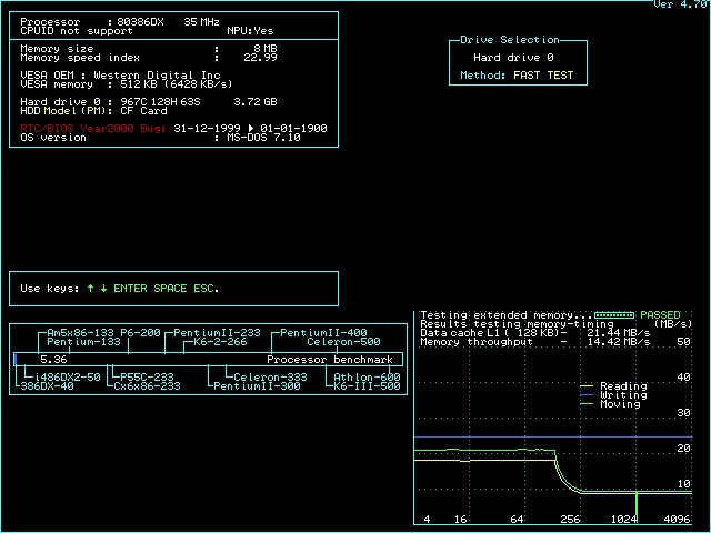
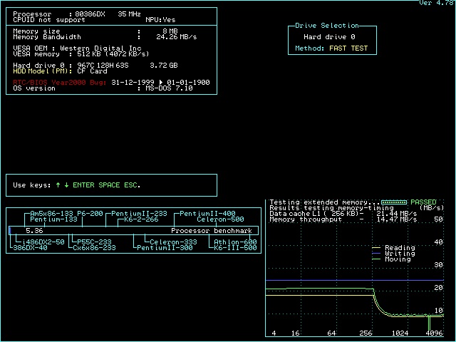
Am386DX-33, SpeedSys v4.78 with 128 KB L2 cache (left), and 256 KB L2 cache (right)
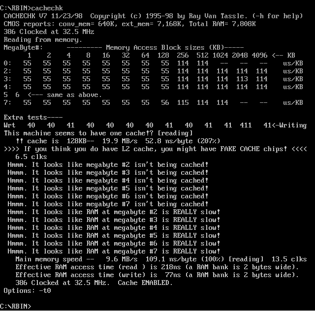

Am386DX-33, CacheChk 7 with 128 KB L2 cache (left), and 256 KB L2 cache (right)
By underclocking the CPU from 40 MHz down to 33 MHz, the memory throughput reduces in line with this - approx. 17% slower. Looking at CacheChk's results, it looks like we've hit a low watermark (under 10 MB/s possibly) with this board/cache's performance and it's assuming no caching is taking place.
The additional cache chips I installed were borrowed from my FIC 486-VIP-IO2 motherboard but these are faster 15ns jobs and to get the most out of this board I want them all to be at this speed.
So I bought ten used 15ns cache chips from Ebay to replace the slower ones that came with the EXP3406. There are numerous articles on the web about fake chips, especially from China, so this was a bit of a gamble. Here is what I received for £11.98 delivered (forgive the pics - I had already installed 5 of them by the time I wrote this!):
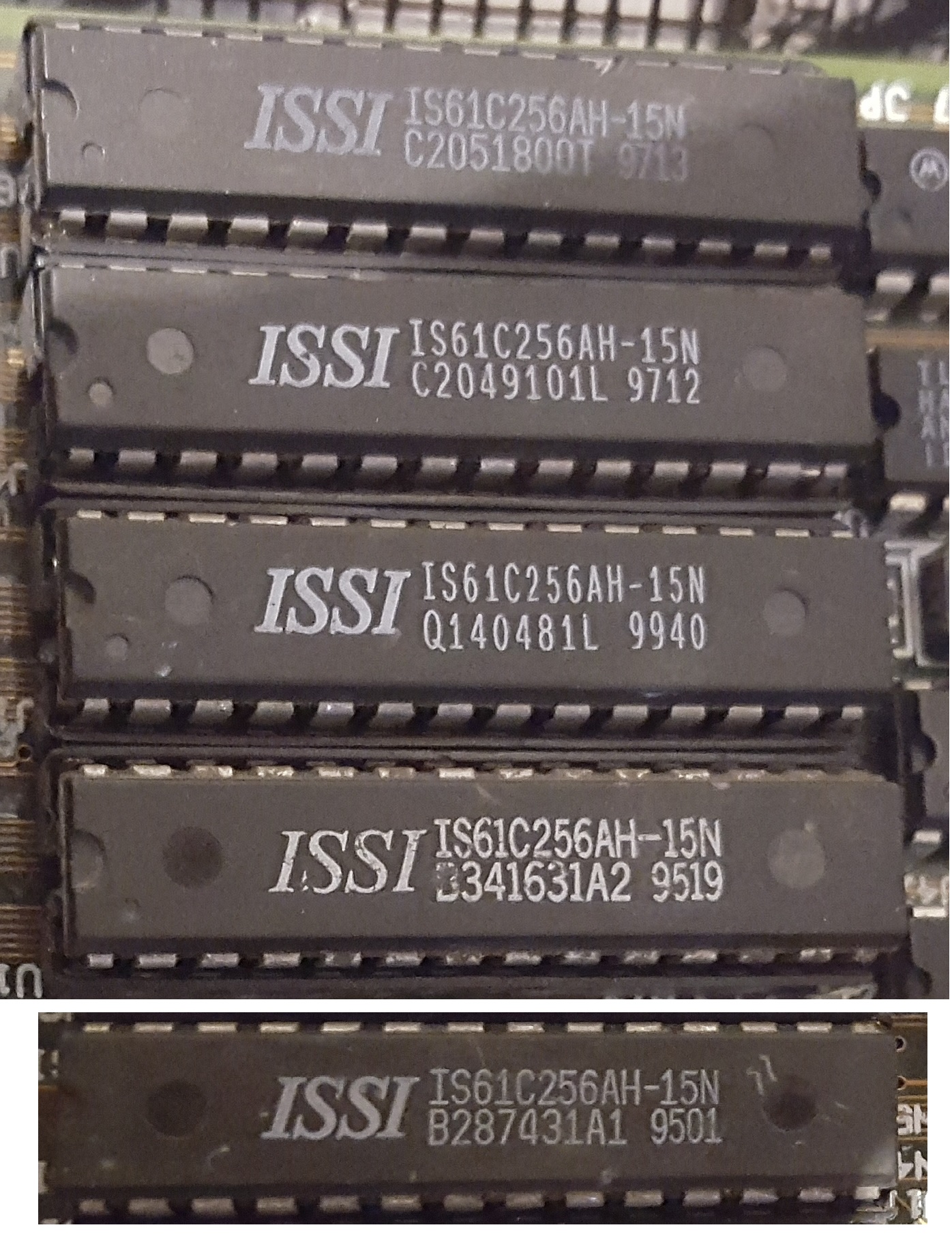

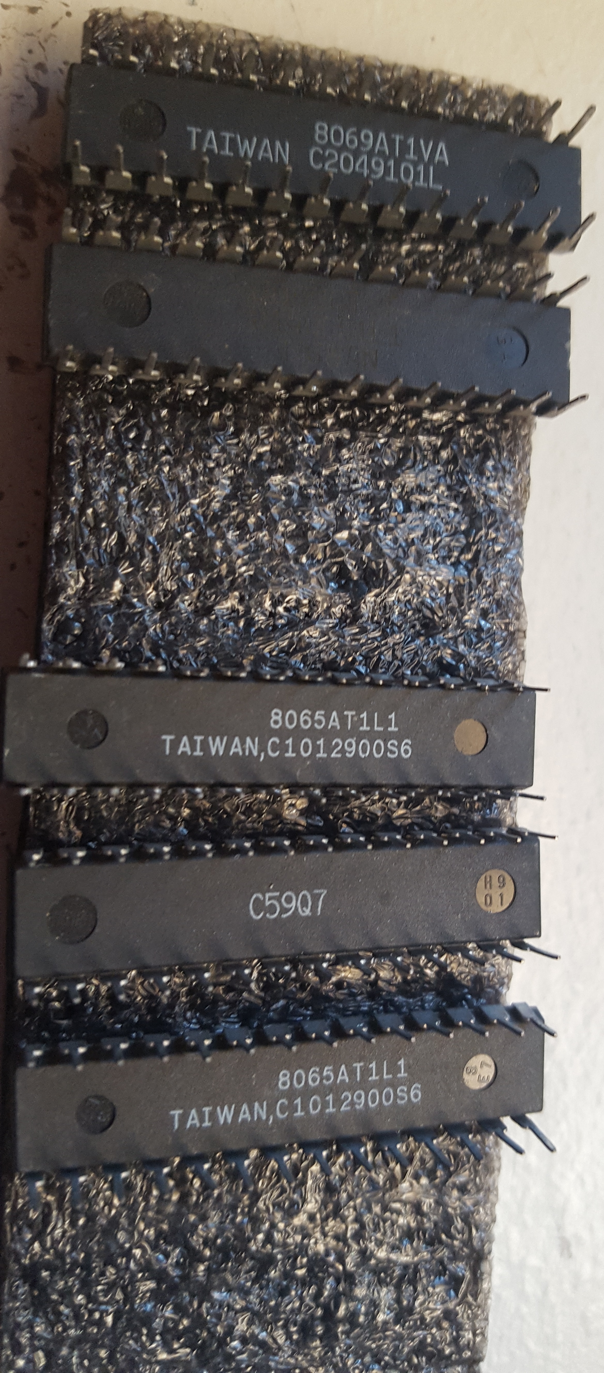
10 ISSI-branded 15ns SRAMs - do they work?
Judging by the state of these, they look like "pulls" from a board. They have some scratches here and there so it's unlikely they have been sanded down and repainted; the logo looks fairly consistent though some chips have a slightly fatter font. Date codes are all over the place, ranging from 1995 to 1999, which is probably also a good sign compared to receiving 10 chips that are all identical. Finally, the legs do not appear to have been re-tinned - they are dull and a bit scratched. Anyway, the only way to know for sure is to test them out!
Having installed 5 of them I discovered the top 2 in the rightmost two images above simply don't work - the machine wouldn't POST. The 5 on the left seem to work just fine - I installed 4 of them in bank 0 and the bottom one replaced a 20ns Samsung in the Tag RAM socket. So the board is now populated with 256 KB of 15 nanosecond L2 cache!
Math Coprocessor
To test an FPU in the larger socket, I installed a Cyrix 83D87-33.
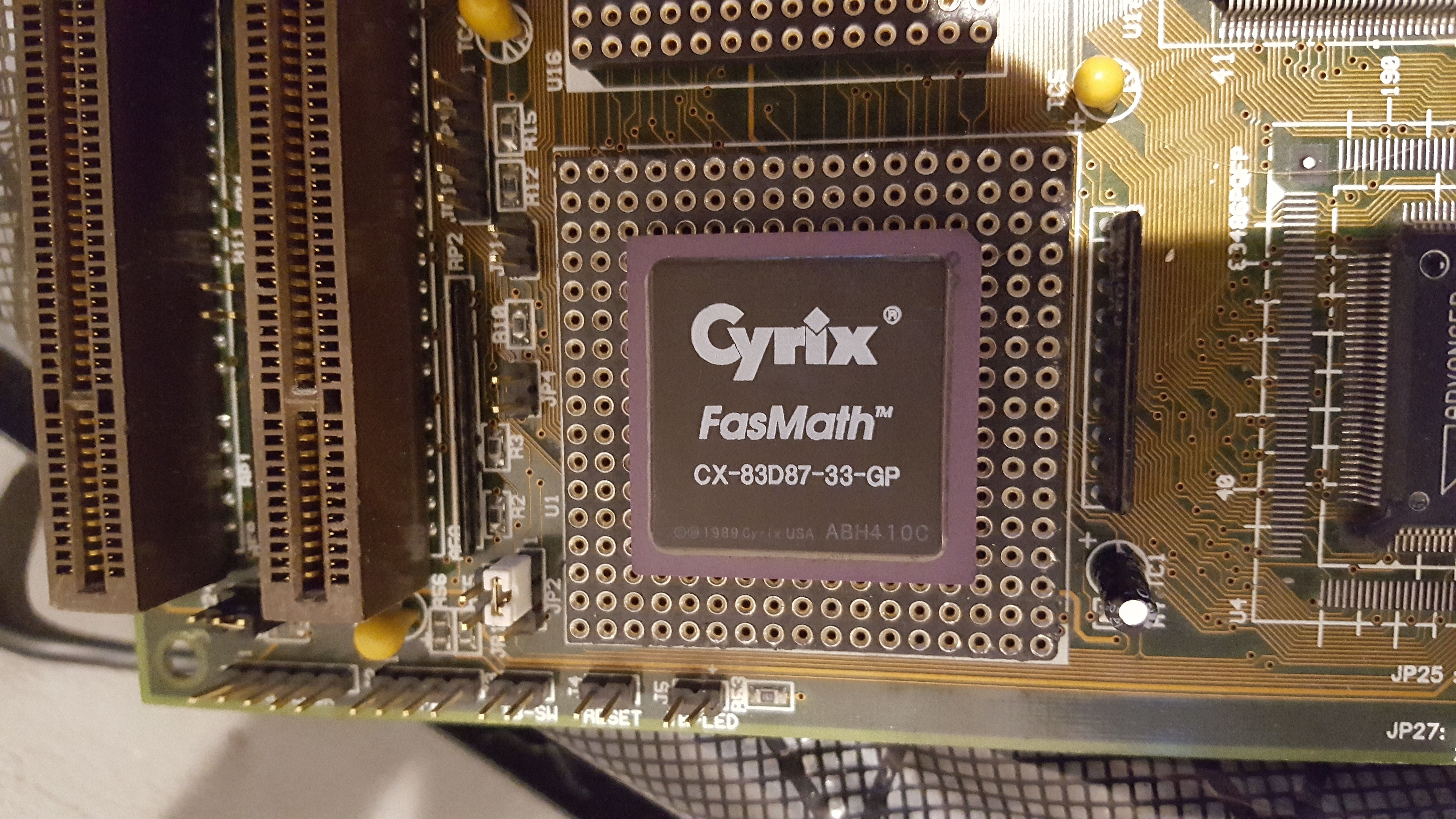
This worked well when I underclocked the Am386DX-40 to 33 MHz. I did try running it at 40 MHz, i.e. overclocking the coprocessor as well to 40 MHz, but while the system booted, graphical glitches soon manifested on the screen to the point I couldn't read anything.
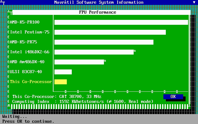
I ran an FPU synthetic benchmark while it was running at 33 MHz and got the following:
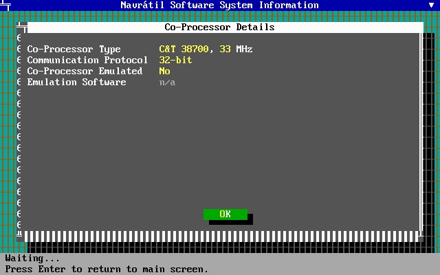
Interesting that it detects my Cyrix CX-83D87 FPU as a Chips & Technologies 38700 - the C&T one, also called "Super Math" is a different design entirely, but is also 100% compatible with the Intel 80387.
Changing the CPU
This is where the real fun will happen... The EXP3406 has two sockets, U1 and U16, that we can use to change the CPU from the AMD Am386DX-40 to something faster (or slower!). Mine only has the one socket but I ordered a PGA-132 socket to solder in. I had to buy 3 for £7.50 delivered.
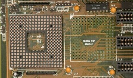
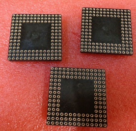
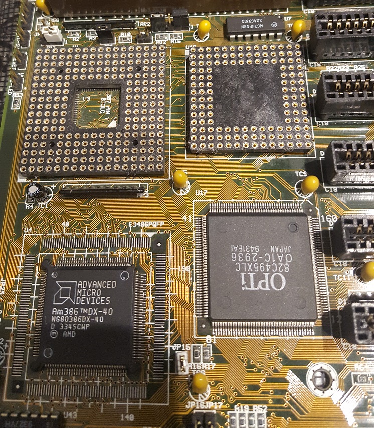
My revision 1.1 did not come with a PGA-132 socket, so I bought one to solder in
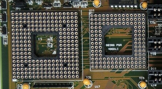
At least one other rev1.1
board I have seen has the upgrade socket, as well as rev1.2 boards
Here's a picture of a revision 1.2 board with the socket fitted. This smaller 132-pin socket is marked '80386 PGA 486DLC' so it is for 80386 CPUs (or 100% compatible), or the Cyrix Cx486DLC, which is really a souped-up 386 with 486SX instructions. It's interesting that this is marked 80386 PGA (Pin Grid Array) as that implies you could fit any 386DX in here, potentially downgrading from the Am386DX-40 to something else! I love motherboards that can span a really long part of the early PC timeline, so I will give that a go just to see if it can! This would mean the board would suit PC gaming from 1985 through to about 1994.
The larger socket (168-pin PGA) is dual-purpose - it can be used to:
a) fit a 387 math coprocessor (using the centre 68 pins only)
-
or -
b) fit an 80486SX, 80486DX, 80486DX-2 or Overdrive (ODPR) CPU
Note the small white triangles in the corner of the sockets - this indicates where you must align pin 1 on the chip into the socket - so when using a CPU in this larger socket pin 1 needs to be in the lower-left corner but if you are installing a 387 math coprocessor into this socket, pin 1 needs to be oriented to the lower-right corner according to the picture above. Pin 1 is usually marked with a dot or dimple in the corner of a CPU, or it has the corner of the chip tapered.
The complete list of CPUs that I believe are supported by this board are:-
- AMD Am386DX 33 (PGA)
- AMD Am386DX 40 (PQFP)
- AMD Am486DX 40 (PGA)
- Cyrix Cx486DLC 33/40 (PGA)
- Intel 80386DX 33 (PGA)
- Intel 80486SX 25/33/40/50* (PQFP or PGA)
- Intel 80486DX 25/33/40/50* (PGA)
- Intel 80486DX-2 50/66* (PGA)
- Intel 487SX (PGA)
- Intel OverDrive 25/33 (PGA)
*plus 5-volt compatibles from Cyrix/IBM/TI/SGS |
Testing the 132-pin upgrade socket
The user manual tells me the jumper settings for '386 mode' seem to allow for only 33 MHz and 40 MHz, so just for fun I set the motherboard jumpers for 33 MHz and tried both an Intel 80386DX-33 and a PGA version of the Am386DX-40. Both worked great.
I also discovered that when in '386 mode', there are some configurations that work but aren't documented in the manual:
| JP6 | JP22 | JP7 | JP8 | |
|---|---|---|---|---|
| 12 MHz | Closed | Closed | Closed | Closed |
| 16 MHz | Closed | Closed | Closed | Open |
| 20 MHz | Closed | Closed | Open | Closed |
| 25 MHz | Closed | Closed | Open | Open |
| 33 MHz | Closed | Open | Open | Closed |
| 40 MHz | Closed | Open | Closed | Closed |
So if you want to underclock your 386DX this gives you the option!
It also supports an Intel 80486SX-2 in both 50 and 66 MHz variants, by selecting the jumpers for 80486SX (PGA), then choosing the 50i setting for speed. The BIOS sees it as a 486DX-50.
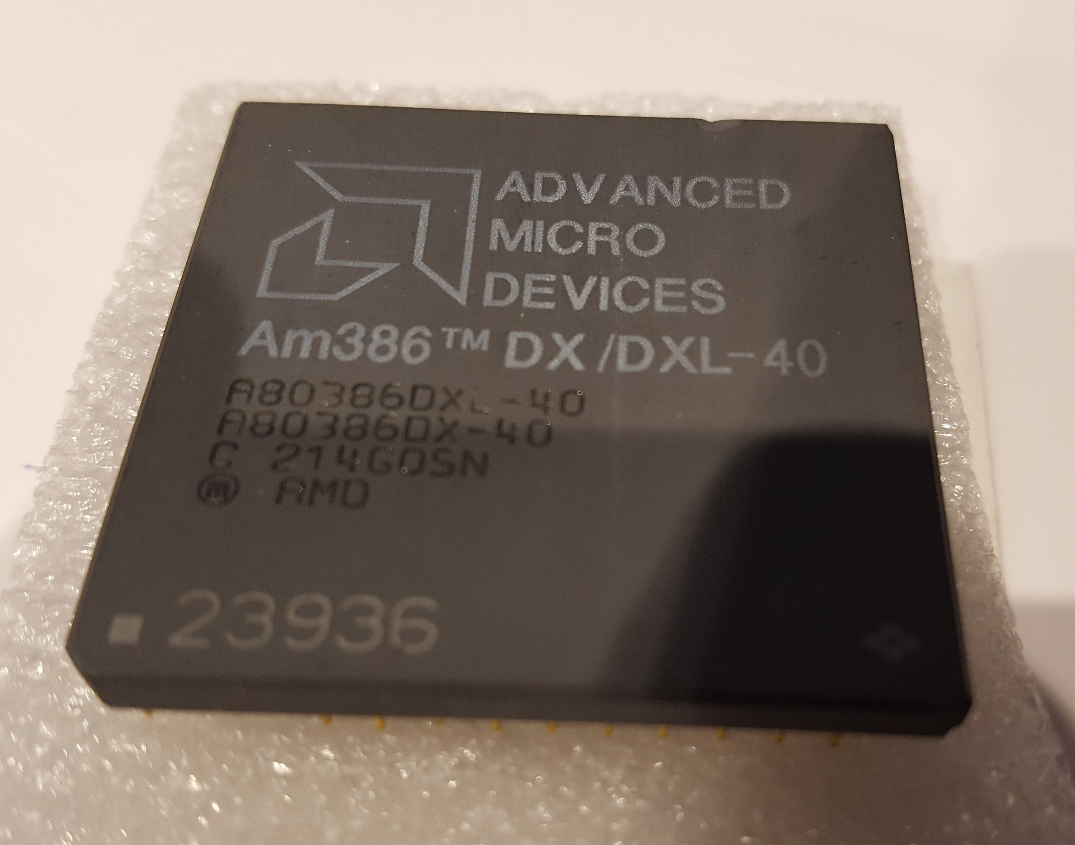

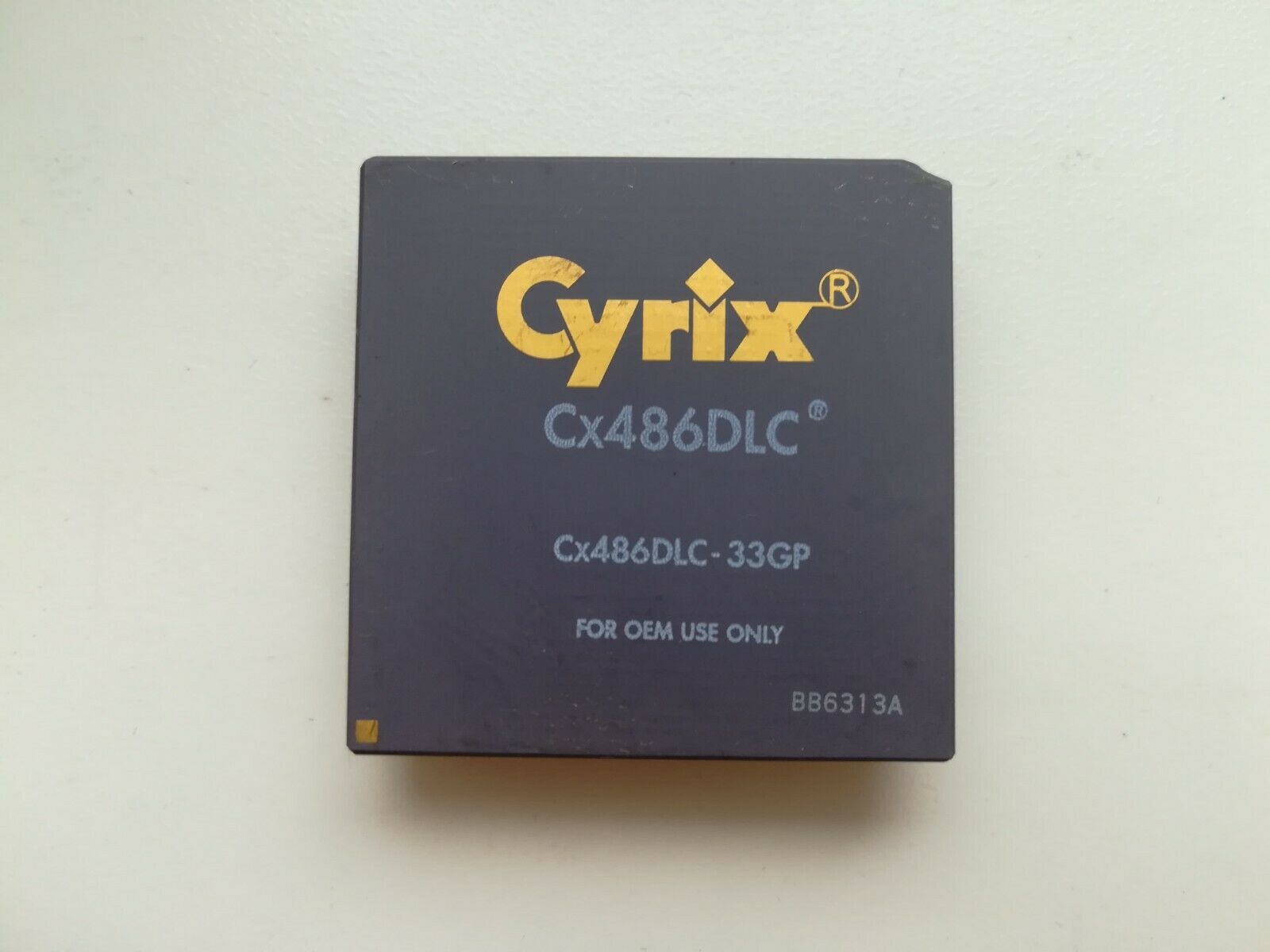
These are my three options for the little 132-pin socket
Well the good news is the new socket I fitted seems to work just fine. I ran 21 benchmarks with the i386DX-33 installed in it, then with a PGA version of the AMD Am386DX-40 (underclocked to 33 MHz to match the Intel), and then without any CPU in the PGA socket so it runs the embedded AMD CPU underclocked to 33 MHz. I'll get to the Cyrix in a bit... Incidentally, there is no way for software to distinguish between an AMD Am386 and an Intel 80386 apart from clock speed (if running the Am386 at 40 MHz, since Intel never released a 386 faster than 33 MHz), so a 33 MHz Intel and a 33 MHz AMD will appear to be identical to the software.
The results can be viewed here.
The first benchmark numbers in the table are with 256 KB of L2 cache enabled. The numbers in brackets are those with the L2 cache disabled. All the above 386 CPU tests were performed with a Cyrix 8C387-33 math coprocessor installed. BIOS settings included 0 wait states for memory read and memory write, and 1 wait state for L2 cache read and write.
As you can see, there is negligible difference when running the embedded (PQFP) Am386DX to running a CPU in the PGA socket.
Now to test the super-special Cx486DLC-33 "upgrade chip". I don't have a 40 MHz version of this CPU, so will use my 33 MHz one instead. With its 1 KB of L1 cache it should give a decent performance boost over the Am386DX-40.
The MR BIOS on this mobo is 'Cyrix DLC aware', and it provides a setting to enable or disable the L1 cache. I double-checked the cache is enabled/disabled by using the Cyrix Cx486DLC utility which allows you to tweak the CPU registers directly, as there have been reports of some 'Cyrix aware' motherboards failing to enable the cache correctly.
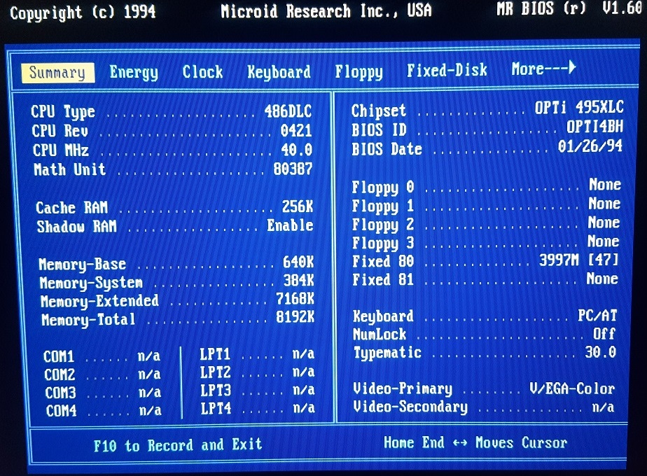
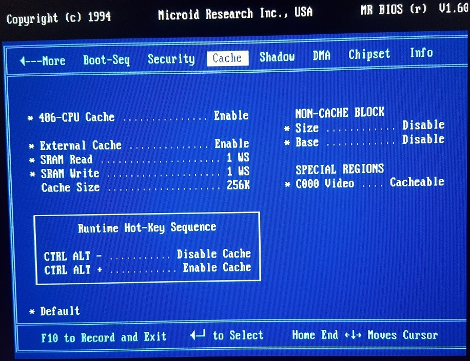
Summary page (left) and Cache page (right)
with Cx486DLC installed
Strangely, SpeedSys v4.78's memory timing chart doesn't detect the 1 KB of L1 cache. CacheChk v7 also fails to detect the L1 cache, but running the "cachecct" tool does show the L1 cache as operational.
The Landmark 2.00 figure of 108.28 looks to be as expected - One of the Cyrix L1 cache utility readme files states that: "A 40MHz Cx486DLC should get 129 on Landmark v2.00 -- the 33MHz part should get about 108. For comparison, an Intel chip [486SX] gets about 110 at 33MHz, 134 at 40MHz and about 167 at 50MHz. Use your favourite benchmark to make sure it is enabled."
Overclocking to 40 MHz
It is often said that Cyrix Cx486SLC and DLC processors do not overclock well, and my Cx486DLC-33 here does run fairly hot without any cooling (another common fact about these chips). Still, I thought I would retest with an overclock to 40 MHz and put a heatsink and fan on to assist with the extra burden. All the benchmark results can be seen in charts and a table at the bottom of this page, but to summarise, overclocking the Cx486DLC to 40 MHz gave an average of 20% performance boost over the stock 33 MHz. Comparing the overclocked Cx486DLC 40 MHz to the embedded Am386DX-40, synthetic benchmarks showed a massive 156% gain (so 2.5x the speed of the Am386DX clock for clock). In Wolfenstein 3D the gain was only 32%, but in Doom the gain was a better 63%, which means I was getting around 15 fps with a fast ISA graphics card.
UMC U5S-Super 40
I also installed my UMC U5S-Super40 CPU on the EXP3406 board. This was detected as a Cx486DLC running at 56.7 MHz. The UMC is a highly optimised version of an Intel 80486SX CPU, offering similar integer performance to an Am486SX2-66 while still being pin-compatible.
Adding a VESA Local Bus Graphics Card
The time period of the EXP3406 motherboard was when graphics cards were starting to be the bottleneck to achieving higher frames per second in the latest games. As CPU clock speeds rose to 66 MHz, it became ever more obvious that running a graphics card via an 8 MHz expansion bus wasn't going to cut it. Enter the VESA Local Bus, which was standardised in 1992. Able to run independently of the CPU's clock (hence the term 'local' in the name), VLB as it was often abbreviated, could run at up to 50 MHz compared to the ISA bus's crippled 8-10 MHz! This gave rise to graphics cards manufacturers producing 'graphics accelerator' cards that could realise much better performance.
When I got this hybrid 386/486 motherboard I only had one VLB graphics card - an Orchid Fahrenheit VA VLB with 1 MB of 70ns RAM. So I purchased another for the purpose of comparative testing here alongside the numerous ISA graphics cards I have. VESA Local Bus graphics cards seem to be going for silly money these days (£50 to £200) for what they are. I really wanted to get hold of a Tseng Labs ET4000/W32 or a Cirrus Logic CL-GD5428, as these are considered very good cards and are relatively common. Fortunately, I was able to find this one and picked it up for £40 shipped in tested/100% working condition:
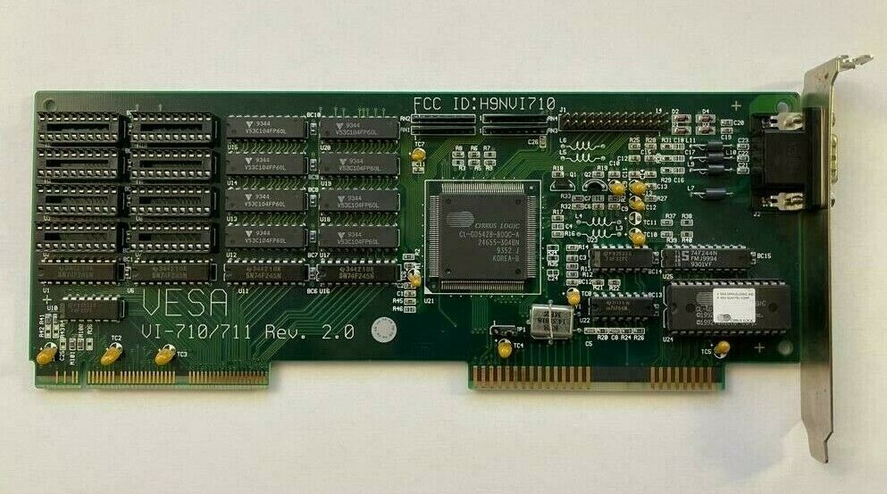
An EliteGroup (ECS) VI-711 SVGA VLB Graphics Card
I have no real knowledge of this card, only that it uses the Cirrus Logic CL-GD5428-80QC-A chipset, and has a spare RAM bank. The RAM chips that are on here are eight V53C104FP60L, which are 256K x 4-bit FPM DRAMs able to run at 60ns RAS access time. This means each chip is 128 KB in capacity, so the board has 1 MB populated. The empty RAM bank is nice, since it means I can upgrade this board up to 2 MB - something that would have been about the maximum in 1993 when the motherboard was produced - though for DOS use most games ran in 320x200 resolution and in 256 colours which requires just 64 KB of video memory. For 640x480 or 800x600 at 256 colours you needed to have 512 KB of video memory. So anything higher really only comes into play for Windows when higher resolutions and/or colour depth are required. Having said that, graphics cards during this time often employed memory interleaving (reading from two or more banks of memory almost in parallel) which was one way performance could be increased greatly so potentially adding more video memory could improve performance too.
One interesting thing I noticed is that Total Hardware 99 / Stason.org show the VI-711 as having a Tseng Labs ET4000 chipset instead of the Cirrus. There was also a revision 3.0 of this same ECS card, though the differences are negligible. There was also a VI-711A which is a lower-profile VLB card running the same Cirrus chipset as mine, but has no memory upgrade capability.
The other ISA-based cards that were used in these tests were:
- Trident TVGA-8900CL-B, 1 MB 70ns RAM, 80 MHz 6-bit RAMDAC
- Cirrus Logic CL-GD510A/520A, 256 KB 120ns RAM, 35 MHz 6-bit DAC
- STB Power Graph w/ Tseng Labs ET4000AX, 512 KB 80ns/100ns RAM, 66 MHz RAMDAC
- STB Power Graph w/ Tseng Labs ET4000AX, 1 MB 70ns RAM, 66 MHz RAMDAC
- Northman Technologies' w/ WD90C30-LR, 512 KB 70ns RAM, 80 MHz 24-bit RAMDAC
All of the above are 16-bit ISA except the Cirrus card which is 8-bit.
Other test hardware
In case you were wondering, while conducting the various tests on this motherboard, I used the following additional hardware:
PSU: Original 1991 vintage Seventeam AT power supply casing upgraded by me with innards from modern ATX PSU + an ATX to AT converter.
Hard Disk Controller: Goldstar Prime 2C 16-bit ISA card (with IDE and FDC connectors)
Hard Disk: CF-to-IDE interface + 4 GB CF card formatted to several FAT16 partitions
Video Card: Several - see results
Keyboard: IBM-branded KB-8296 "AT" 102-key enhanced keyboard.
All Benchmark Results
This section summarises all the results gathered from 386DX-25 up to 486DX2-66 on the EXP3406 motherboard.
I'm going to jump to the end and show you a comparison of all the CPUs in the test. By adding up all the benchmark results together for each CPU we can get a visual representation of how they all compare:
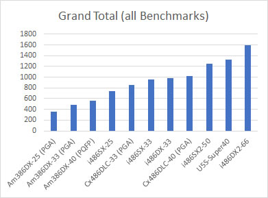
The clock-doubled CPUs are of course the fastest here along with the UMC 40 MHz which gets its bump in speed via internal efficiencies over Intel's design. The Cyrix Cx486DLC-40 "upgrade" processor takes a distant 4th place, much more on par with the Intel 486-33s.
Synthetic Benchmark Test Results
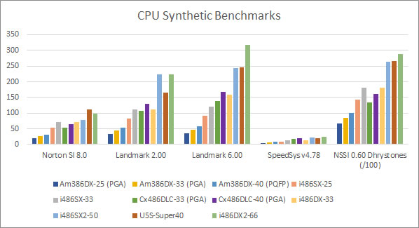
Click on the chart to display a larger version with data values displayed
For more "real world" testing (games and 3D), we have six sets of benchmark results. 3DBench 1.0 for slower computers and 1.0c for faster computers (though this is of greater benefit on Pentiums and beyond), Chris' 3D Benchmark, PC Player benchmark, and timed demos from Wolfenstein 3D and Doom.
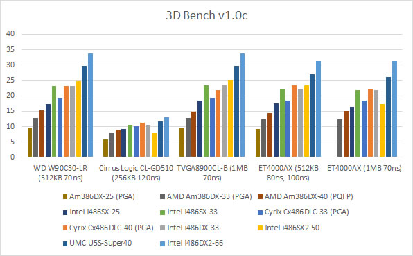
3D Bench v1.0 / v1.0C
Starting with 3D Bench v1.0, also known as the Superscape Benchmark, the Cyrix Cx486DLC-40 stands up well against an Intel 486 at 33 MHz on most video cards. The CL card shows its bottlenecking 8-bit ISA bus, as the 386 and 486 are so closely-matched. The UMC U5S Super40 is an awesome chip considering it's not clock-doubled and was very cheap to buy!

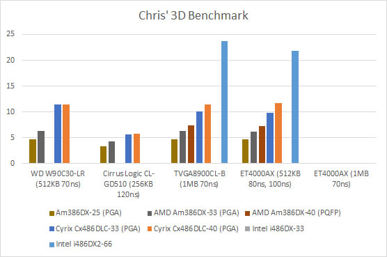
Chris' 3D Benchmark
Chris' 3D Benchmark only works on machines that have a math coprocessor, so we can rule out all the SX units from our tests. The results show how much clock-doubling improves the performance on this benchmark.
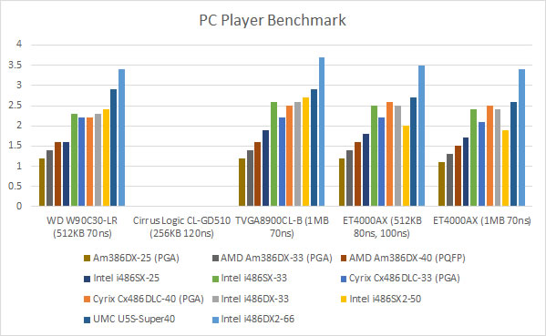
PC Player Benchmark
PC Player was run using the default VESA mode 100, which is 640 x 400 x 8 bits per pixel. The exception to this was the Western Digital card which did not have mode 100, so mode 101 was used instead (640 x 480 x 8 bpp).
Wolfenstein 3D Timedemo
Moving onto the games, unsurprisingly, the 486DX2-66 leads in the Wolfenstein 3D time demo (Episode 1, Level 1), but not by much. What is more interesting is we see the UMC chip in a solid 2nd place, and in most cases only slightly behind the DX2-66. In third are the 486SX and 486DX running at 33 MHz. The Cyrix chips show that clock for clock they lag behind their Intel cousins, but having the 40 MHz variant helps it keep pace with the 33 MHz Intel on most graphics cards.
The much-liked Am386DX-40 comes in similarly to the Intel 486SX-25 for most cards giving a steady 25+ frames per second. This is not far behind the Cx486DLC-33 which usually is just 3-5 fps faster. I'm not too sure why the Trident and 512 KB ET4000 got very different results here.

Doom Timedemo
In the Doom timedemo benchmarks, you can see the Western Digital card leading the pack with an average of 25.2 frames per second on the DX2-66. For any ISA graphics card, this is about the fastest you will see. The game automatically limits FPS to 35 anyway. Having more than 512 KB of video memory doesn't make any difference as both 1 MB cards show. What does make a difference is clock speed.
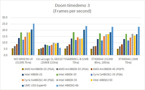
Because Doom does not make use of a math coprocessor, having a DX over an SX gives no benefit. The slight FPS differences when comparing 486SX-33 and 486DX-33 are due to slightly different BIOS settings (cache timings). The Trident card is [rather oddly for them] a solid performer though is let down by its inability to run on an overclocked ISA bus. If it weren't for this, it would be slightly faster than the ET4000. Of course, the Cirrus Logic card brings up the rear due to its 8-bit bus. The Western Digital again proves itself to be an excellent ISA card. One consistent surprise is the 1 MB ET4000 being slower than the 512 KB variant (same card, 70ns RAM taken off the Trident card).
Sadly, the Cyrix Cx486DLC's performance was not great, sitting between an Intel 486SX-25 and -33. Doom is playable, but only just. These days it is recommended playing Doom on a Pentium-class system for smooth 35 fps throughout.
Conclusion
So how does the Data Expert EXP3406 compare to other motherboards of similar era? If using an ISA graphics card, the fact you can overclock the ISA (AT) bus quite substantially gives it great performance if your cards can handle the added speed. The VESA Local Bus should provide a huge bump in graphics performance, but my tests showed they only marginally bettered the fastest ISA cards and in some cases performed a little worse! This implies that something else was the bottleneck, not the graphics cards. I would say this board is ideal for DOS gaming where the sweet spot is a 40 MHz CPU or slower, but after this point you are starting to get into VLB/PCI graphics cards and faster 72-pin SIMM memory, and at that point it gets left behind pretty quickly.
Thanks for following along on this review - let me know if you have ideas on further testing!
Smallprint on each of the CPUs Tested and BIOS Options
Only a handful of BIOS settings were changed throughout the test runs. They are:
- Cache Burst Cycle
- SRAM [Cache] Read Cycle
- SRAM [Cache] Write Cycle
- DRAM Read Wait States
- DRAM Write Wait States
- AT Bus Clock
Cache Burst Cycle
When using a 486-class CPU, this option becomes available since the 80486 and compatibles have what is called 'Burst Mode'. There are four cache "timings" available in the MR BIOS, which are: Fast 2-1-1-1,
Med 2-2-2-2,
Med 3-1-1-1 and
Slow 3-2-2-2. The first digit indicates how many CPU cycles the system will take to read the first 32 bits. The next three digits indicate how many CPU cycles the system will take to do subsequent reads. So 2-1-1-1 is the fastest (if your machine can keep up), while 3-2-2-2 is the slowest.
SRAM Read Cycle
This denotes how many wait states the board will put in when reading from the L2 cache.
SRAM Write Cycle
This denotes how many wait states the board will put in when writing to the L2 cache.
DRAM Read Wait States
This denotes how many wait states the board will put in when reading from main memory.
DRAM Write Wait States
This denotes how many wait states the board will put in when writing to main memory.
AT Bus Clock
The 82C495XLC generates the AT bus clock (ATCLK) from
an internal division of CLK (called 'CLKI'). The ATCLK frequency is programmable
and can be set to any of four clock division
options, which are ATCLK/3, ATCLK/4, ATLCLK/5 and ATCLK/6. Essentially this means the ISA bus (aka AT bus) can be run at speeds from 5.6 MHz up to 13.3 MHz. The traditional speed of the ISA bus is 8 MHz, so overclocking the bus can often cause instability if an expansion card cannot handle running at faster speeds.
CPU Setup
Am386DX-40
Norton SI reports the Am386DX-40 scoring 31.2 with the L2 cache enabled, and 15.6 with it disabled. Strangely, this scores the AMD chip slower than a standard Intel 80386DX-33, which apparently comes in at 35.9, though I haven't tested that. My advice is don't take any one benchmark in isolation.
I then went into the BIOS and changed the L2 cache wait states from their defaults of 1 WS (both read and write) to 0 WS on both, and retested. Now Norton SI is returning a figure of 43.2 with the cache enabled.
SpeedSys v4.78 returns a score of between 8.38 and 9.33 which puts this system on par with an i486SX-25. With 1 WS on cache write, 0 on read and main memory both on 0 WS, it gave my 8 MB of 70ns memory a bandwidth of 24.39 MB/s. With the Orchid Fahrenheit VA VLB graphics card it said my VESA memory bandwidth was 4600 KB/s. The extended memory throughput came out at 27.44 MB/s for the 256 KB of L2 cache and 16.61 MB/s for main memory.
NSSI reported an average of 11,947 Dhrystones/second for the CPU, and 663 KWhetstones/second for the software-emulated FPU.
CacheChk v7 correctly identified the 128 KB of L2 cache on the motherboard, giving a cache throughput of 27.6 MB/s and a main memory speed of 10.6 MB/s (99.1 ns/byte), with an average read access time of 198ns and average write access time of 64ns.
Cyrix Cx486DLC-40
With the Cyrix Cx486DLC-40 (well, DLC-33 overclocked to 40 MHz), I only modified three settings from the default. Both memory wait states were dropped to 0, and the ISA bus was boosted to 13.3 MHz. This all ran very stable throughout the testing process with one exception: the Trident card would hang on Chris' 3D benchmark at 13.3 MHz - it worked when brought back down to 8 MHz.
Since these CPUs run hot, for peace of mind I put a heatsink and fan over the CPU for most of the time, though without it fitted I can just about keep a finger on the top of the chip all the time.
Intel 80486SX-25
With the Intel 80486SX-25, by default the BIOS sets the Level 2 cache's SRAM Burst Read to "Fast (2-1-1-1)" and SRAM Write Cycle set to 1 WS. Unfortunately, with 256 KB of 15ns SRAM chips, this does not POST. The eventual fastest stable setting I found was "Med (3-1-1-1)" with 1 WS on the SRAM Write Cycle. Memory wait states were both overridden to run at 0 WS (the default is 1 WS), just like I did for the Am386DX-40. I also ran the ISA bus at a slightly overclocked 8.3 MHz.
Norton SI came in at 54.0 which is a healthy 73% increase over the Am386DX-40, and a 108% increase over the Am386DX-33. That's what the 486's 8 KB of Level 1 cache and burst mode gives you!
SpeedSys v4.78 came in at 9.11, so a much more modest 9% gain over the Am386DX-40.
CacheChk v7 correctly identified the 8 KB of L1 cache in the CPU, but failed to identify the L2 cache on the motherboard. The L1 cache throughput came out at 25.4 MB/s. Main memory speed of 14.4 MB/s (72ns/byte), with an average read access time of 291ns and average write access time of 208ns.
Intel 80486SX-33
With the Intel 80486SX-33, I was able to run the cache at "Fast (2-1-1-1)" with 0 wait states. Memory wait states were both overridden to run at 0 WS (the default is 1 WS), just like I did for the Am386DX-40. I also ran the ISA bus at an overclocked 11.1 MHz.
Intel 80486SX2-50
With the Intel 80486SX2-50, the BIOS showed its first failed detection: it saw it as a 486DX-50 (CPU ID 045B). The fastest stable cache settings were unsurprisingly the same as for its non-clock doubled brother, the 80486SX-25 - "Med (3-1-1-1)" with 1 wait state on SRAM Write Cycle. As usual, memory wait states were both overridden to run at 0 WS (the default is 1 WS). I also ran the ISA bus at a greatly overclocked 16.7 MHz! Time will tell if this is long-term stable but it ran just fine for several hours on all cards apart from the Trident that needed this reduced to 8.6 MHz to run the Doom timedemo.
UMC U5S-Super40
This CPU was one I purchased back in the day as a cost-effective upgrade from my Intel 486SX-25. In the tests here, the chip was detected by the BIOS as a Cyrix Cx486DLC running at an odd 57.6 MHz. The SRAM settings default to 1 WS for read and write, main memory wait states are 2 WS for read and 1 WS for write. The AT bus has some crazy options: 9.5 MHz being the slowest, 11.3, 14.2 and a ludicrous 18.9 MHz. Amazingly the system booted at this fastest speed, though any 3D tests crashed early. The test results I logged were for 0 WS on SRAM read and write, and 0 WS on main memory read and writes. The AT bus was set at 11.3 MHz which was stable throughout, apart from the Trident card that needed the lowest setting of 9.5 to work..
With these settings 3DBench got 34.4, Wolf3D's timedemo got 47.9 fps and Doom's timedemo came in at a very respectable 24.5 fps using the Western Digital 512 KB 16-bit ISA video card.
Intel 80486DX2-66
With the Intel 80486DX2-66 tests, the BIOS settings defaulted to "SRAM Burst Read" set to Slow (3-2-2-2) and SRAM Write Cycle set to 1 WS. The system would not POST with the L2 SRAM Burst Read set to Fast (2-1-1-1), nor when set to "Med (2-2-2-2) 1 WS".
The fastest stable setting was "Med (3-1-1-1) 1 WS". Overriding the memory wait states to 0 WS ran fine, as did overclocking the ISA bus to 11.1 MHz (all except the Trident card that wouldn't even run stable at 8.4 or even 6.7 MHz - I had to get it right down to 5.6 MHz to run the Doom timedemo!).
Norton SI returned a figure of 99.0. SpeedSys came in with a score of 24.14. NSSI reported an average of 28,561 Dhrystones/second for the CPU, and 10,953 average KWhetstones/second for the built-in FPU.
CacheChk v7 correctly identified the 8 KB of L1 cache in the CPU as well as the 128 KB L2 cache on the motherboard. The L1 cache throughput came out at 67.5 MB/s (15.5 ns/byte) and the L2 cache throughput was 32.4 MB/s (32.4ns/byte). Main memory speed of 10.9 MB/s (96ns/byte), with an average read access time of 384ns and average write access time of 154ns.

