 Paradise / Western Digital
Paradise Computers was a graphics chipset manufacturer for the IBM PC and its compatibles. It was formed by Paul Jain in 1982 who went on to form Video Seven a few years later. Toshiba used a Paradise VGA chipset in its 1989/1990 range of laptops, including the T3100SX, T3200SX, T5100/100, T5100/200, as did NEC in its PowerMate laptop range and Compaq in its Portable 386.
Paradise were bought out by Western Digital in 1986 and rebranded Western Digital Imaging. This part of the company was then sold in 1991 to Philips (see press release).
Here is a list of their cards in chronological order by bus type:
| ISA Cards | VLB, AGP and PCI Cards |
|---|---|
| Modular Graphics Card (MGC) (1984) PVC4 (1985) Color/Mono Card (1986) AutoSwitch EGA (1986) PEGA 1A / AutoSwitch EGA 350 (1986) PEGA 2A / AutoSwitch EGA 480 (1987) PVGA Plus / WD90C90 (1987) PVGA 1A (1988) Basic (1989?) WD90C00 (PVGA 1B) (1989) WD90C10 (PVGA 1M) (1989) WD90C11 (1989) WD90C12 (1990) WD90C22 (1991) WD90C30 (1990) VGA 1024 (1991) WD90C31 (1992) |
WD90C33-ZZ (1993) WD90C24 (1994) Pipeline-PCI 8 / Pipeline 64 (1995) Bahamas 64VL (1995) |
|
|||||||||||||||||||||||||||
|
|||||||||||||||||||||||||||
|
|||||||||||||||||||||||||||
|
|||||||||||||||||||||||||||
|
|||||||||||||||||||||||||||
|
|||||||||||||||||||||||||||
|
|||||||||||||||||||||||||||
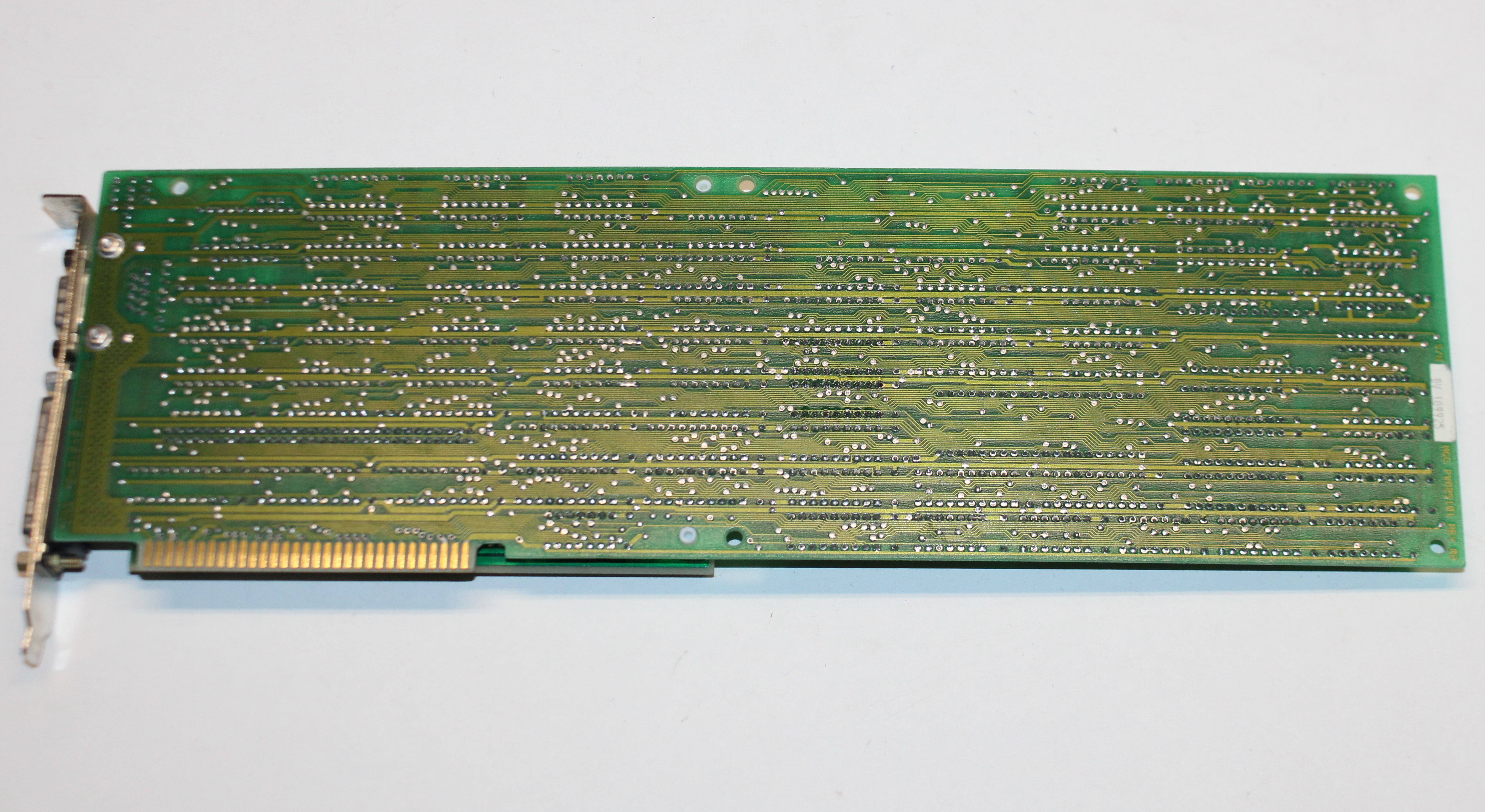
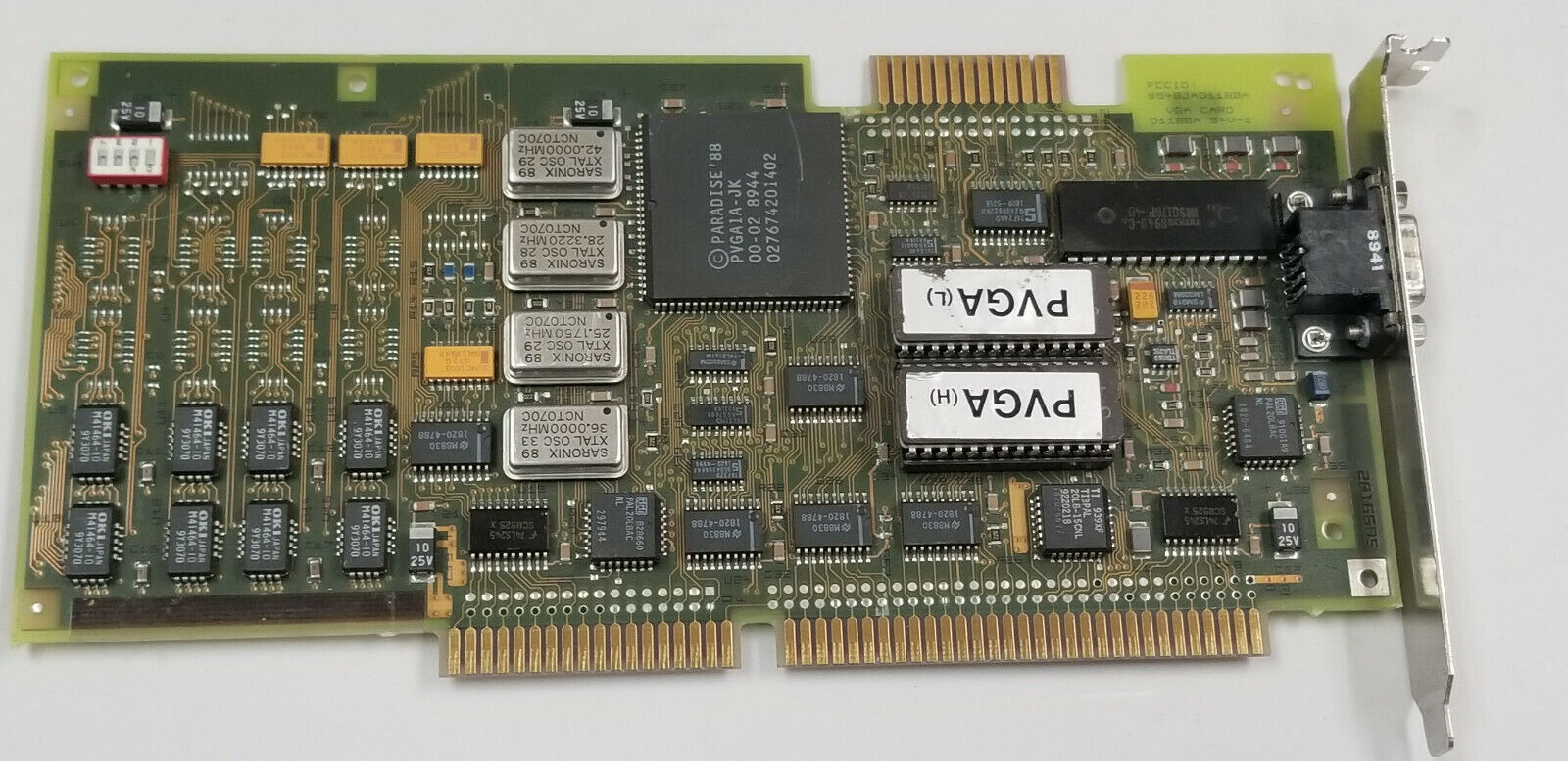
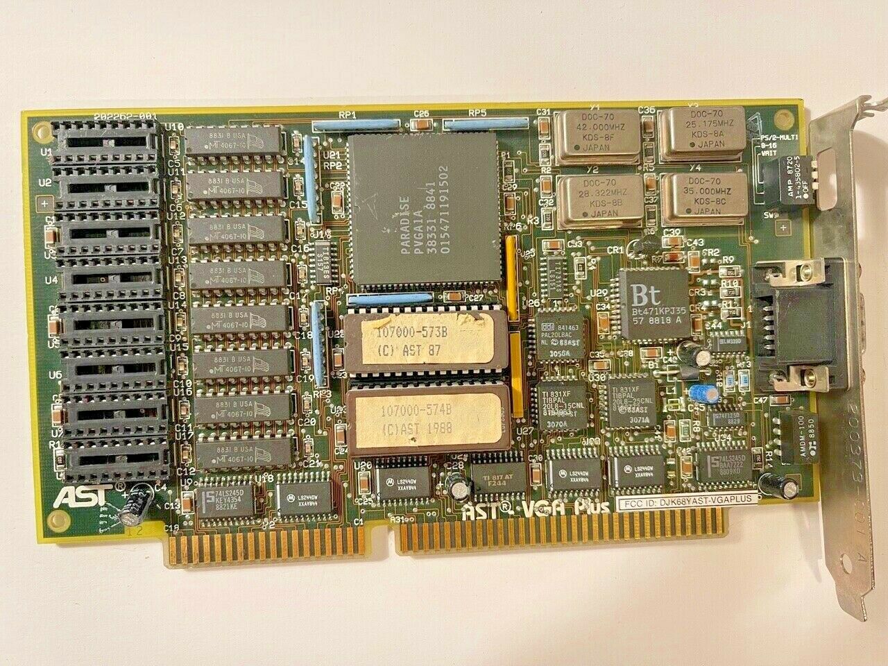
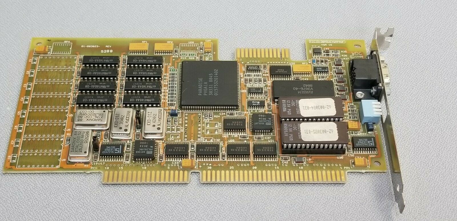
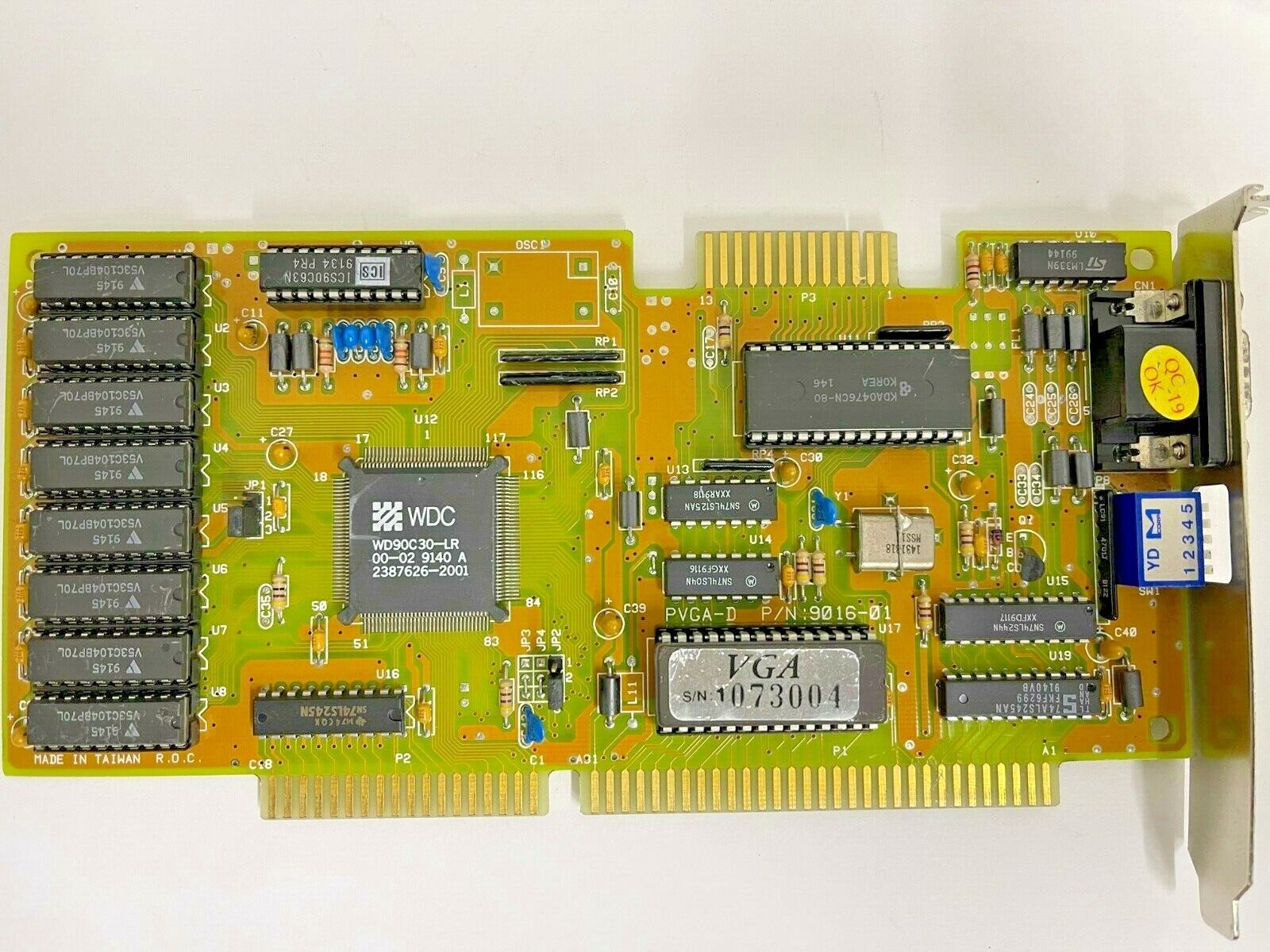
PVGA Plus (WD90C90)
|
|||||||||||||||||||||||||||
|

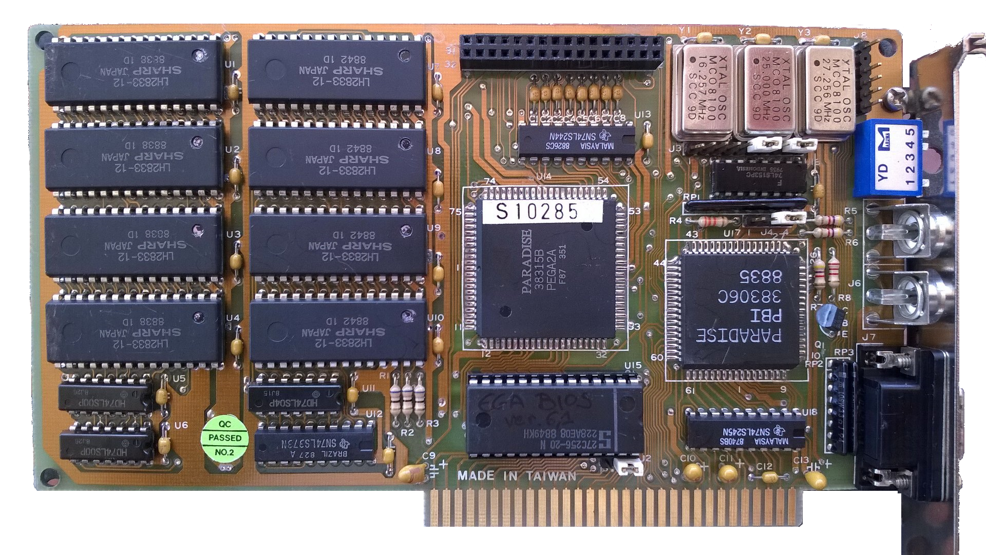
| Configuration | Total Memory | Maximum Resolution and Colours |
|---|---|---|
| Eight 64Kx4 DRAMs | 256 KB | 800 x 600 in 16 colours, or 640 x 400 in 256 colours |
| Sixteen 64Kx4 DRAMs | 512 KB | 1024 x 768* in 16 colours(?), or 640 x 480 in 256 colours |
| Eight 256Kx4 DRAMs | 1 MB | 1024 x 768* in 16 colours(?), or 800 x 600 in 256 colours |
So if you have only eight DRAM sockets on your card, it will not support 512 KB of video memory, only either 256 KB or 1 MB.
The DIP switch settings are as follows:
| SW | Meaning | Description |
|---|---|---|
| 1 | Monitor Type | ON: Multi frequency OFF: Standard VGA |
| 2 | VGA Mode Switching Style | ON: PS/2 Style - All modes available
on all monitors OFF: PC/AT Style - color on color, mono on mono |
| 3 | Not used | Set to OFF |
| 4* | 8bit vs 16bit AutoSense | ON: Auto sense 8- or 16-bit
BIOS access OFF: Force 8-bit BIOS access |
*SW4 not used on VGA Plus.
For my findings on the crystal oscillators on PVGA1A cards, see the section at the bottom of this page called Paradise/WD Crystals.
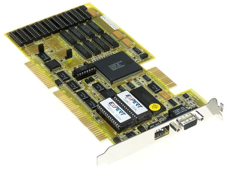
Paradise/Western Digital also shared the PVGA1A with Video 7 who marketed it as their VEGA chipset. After Western Digital's buyout of Paradise, the PVGA1A was rebranded as the WD90C00.
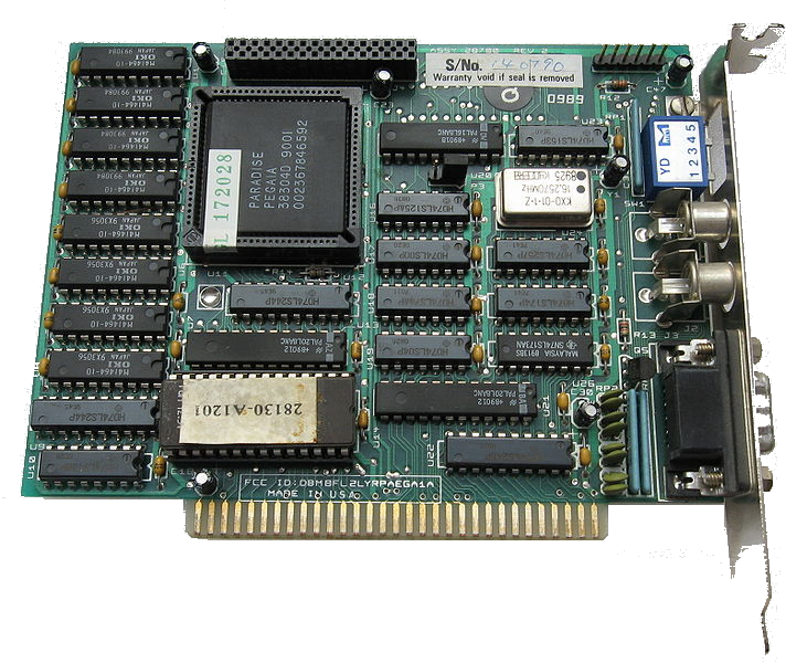
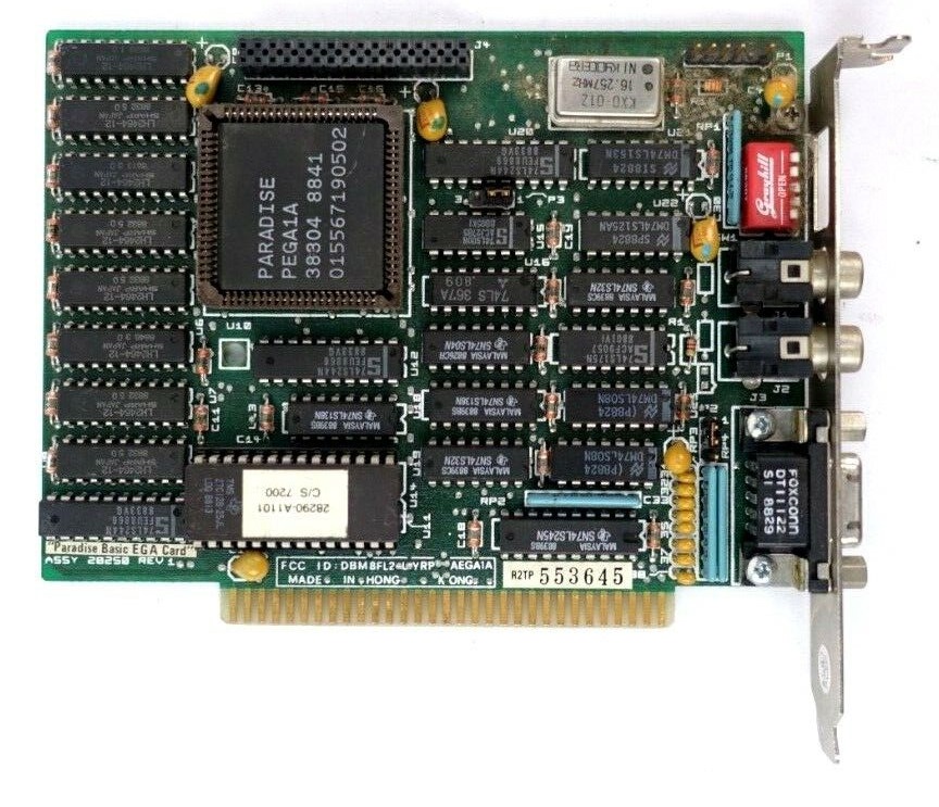
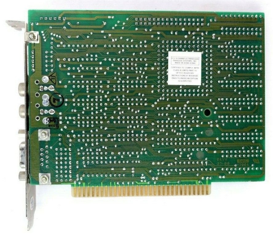
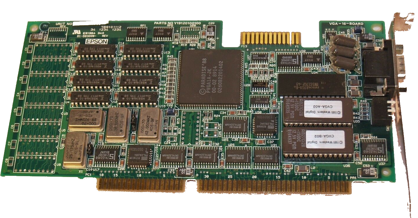
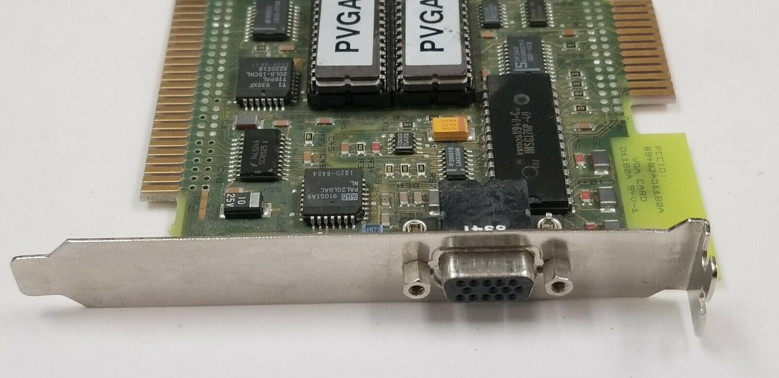
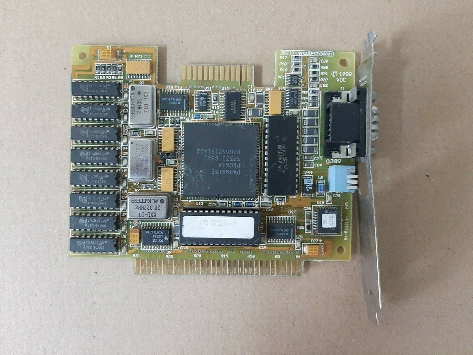
A Seiko/Epson-branded PVGA1A can be seen in the top image and first 2 images below, with FCC ID BKME02V01.
Row 2 is an HP-branded PVGA1A with FCC ID B948JAD1180A (presumably the model number is D1180A).
Row 3 is an AST VGA Plus MXB41.
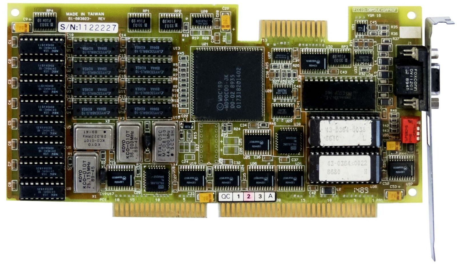
Row 4 is a Philips card with FCC ID DBM5UEVGAPROF. This was also branded as the Expert TopVGA 2100.
Row 5 is a 256 KB Philips card with FCC ID DBM5VEP52V00001
Click here for the PVGA1A datasheet from October 1990.
Click here for another very similar PVGA1A datasheet (also from October 1990).
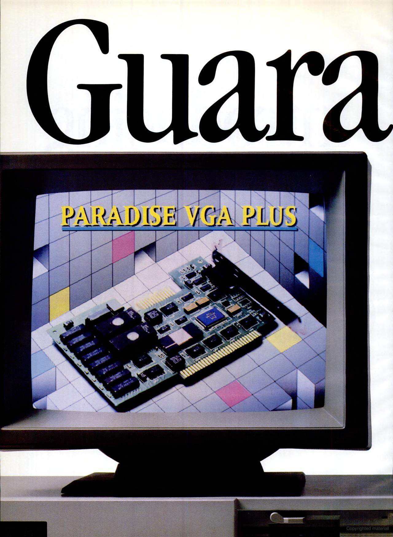
Paradise Advert (1991)
Paradise VGA Plus Brochure
Paradise VGA Plus 16 Brochure
ROM Dump for DBM5VEP52V00001.
Also check out the Paradise Downloads page.
More Images
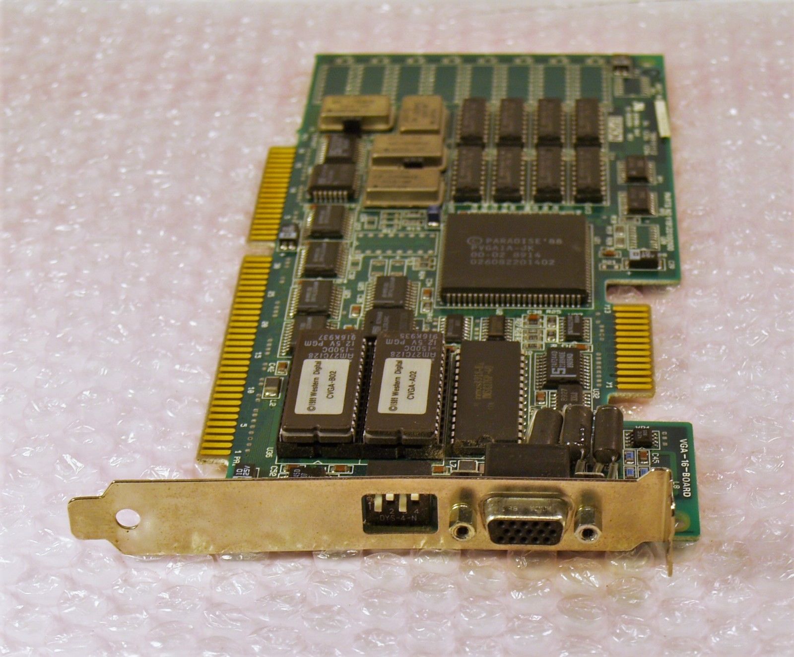
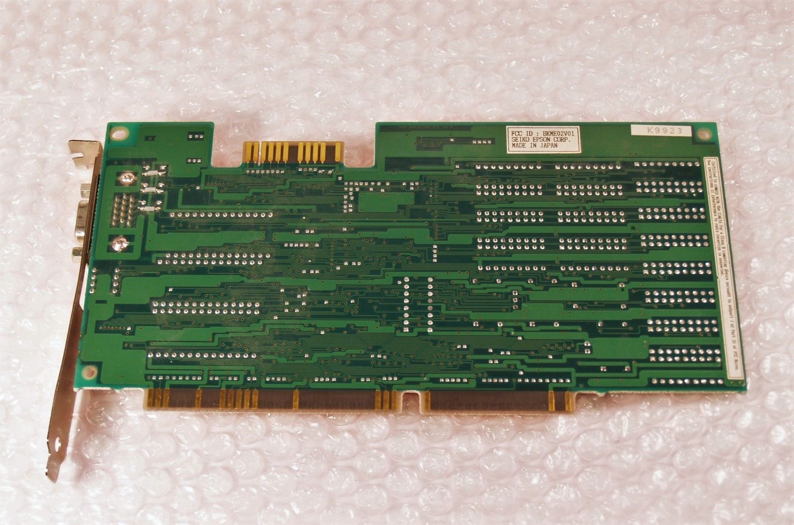
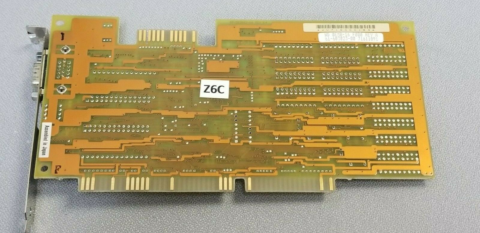
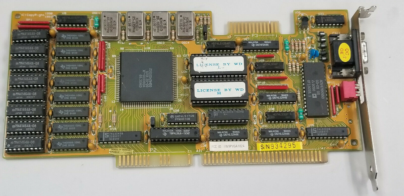
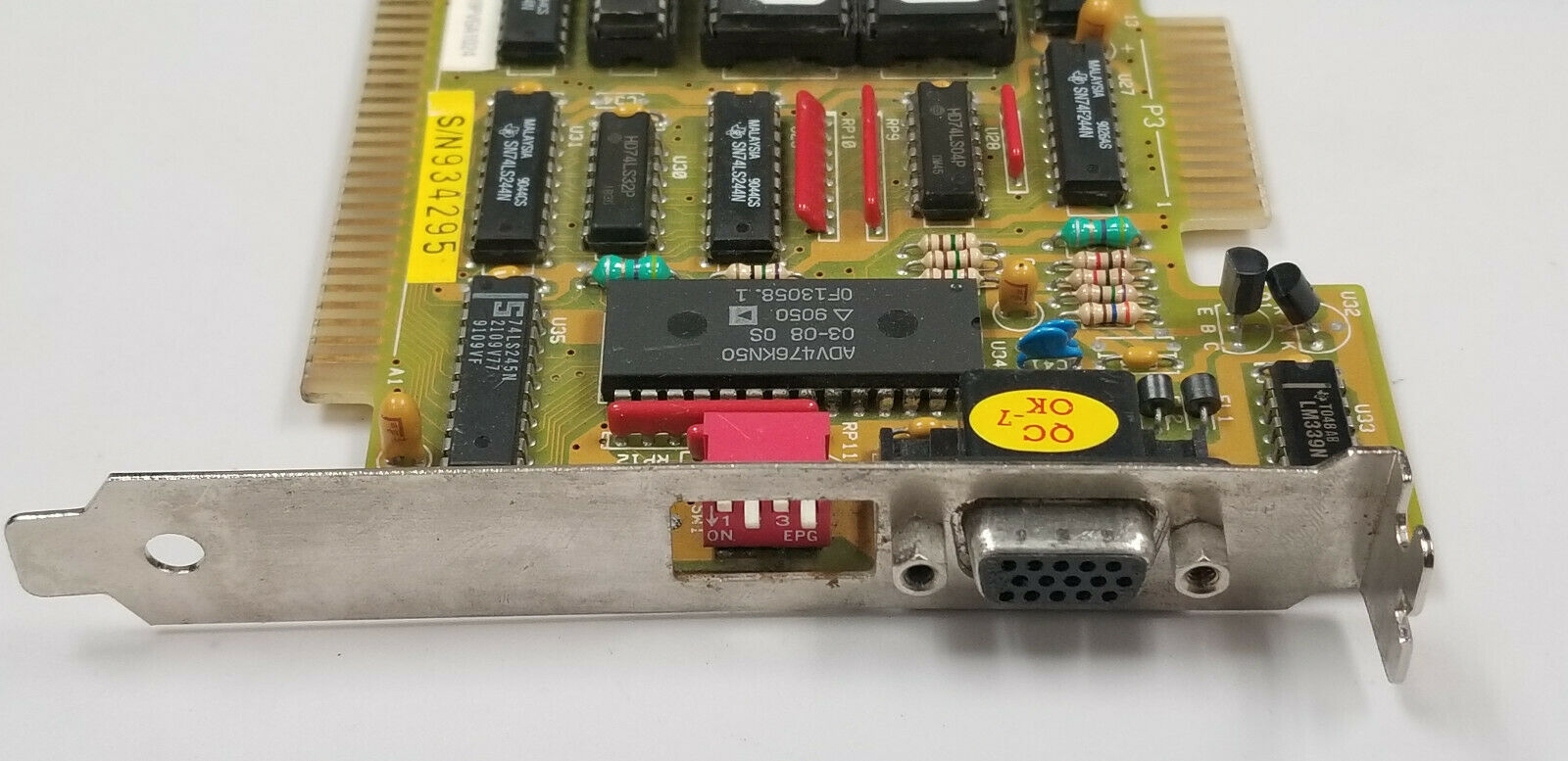
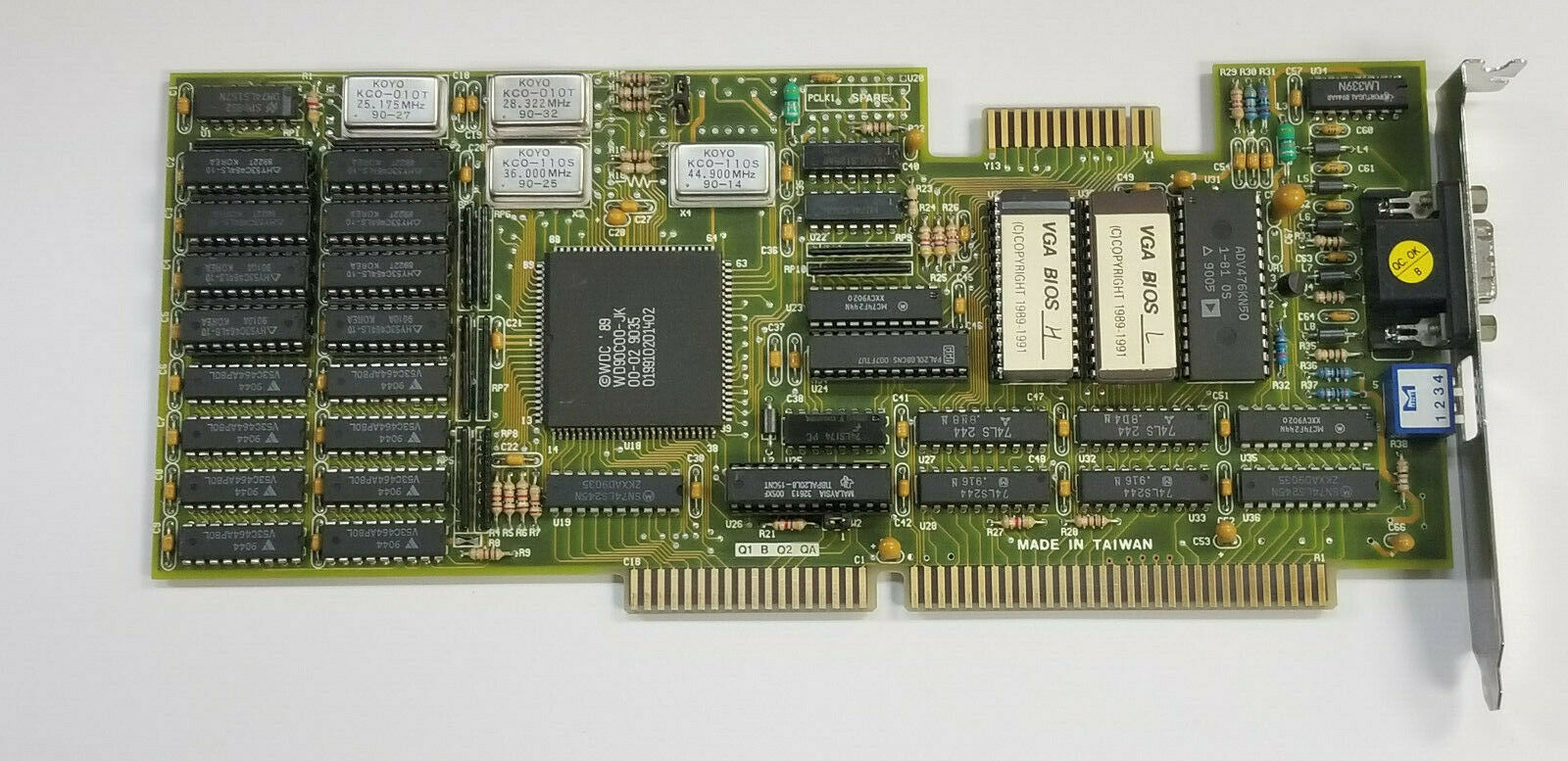
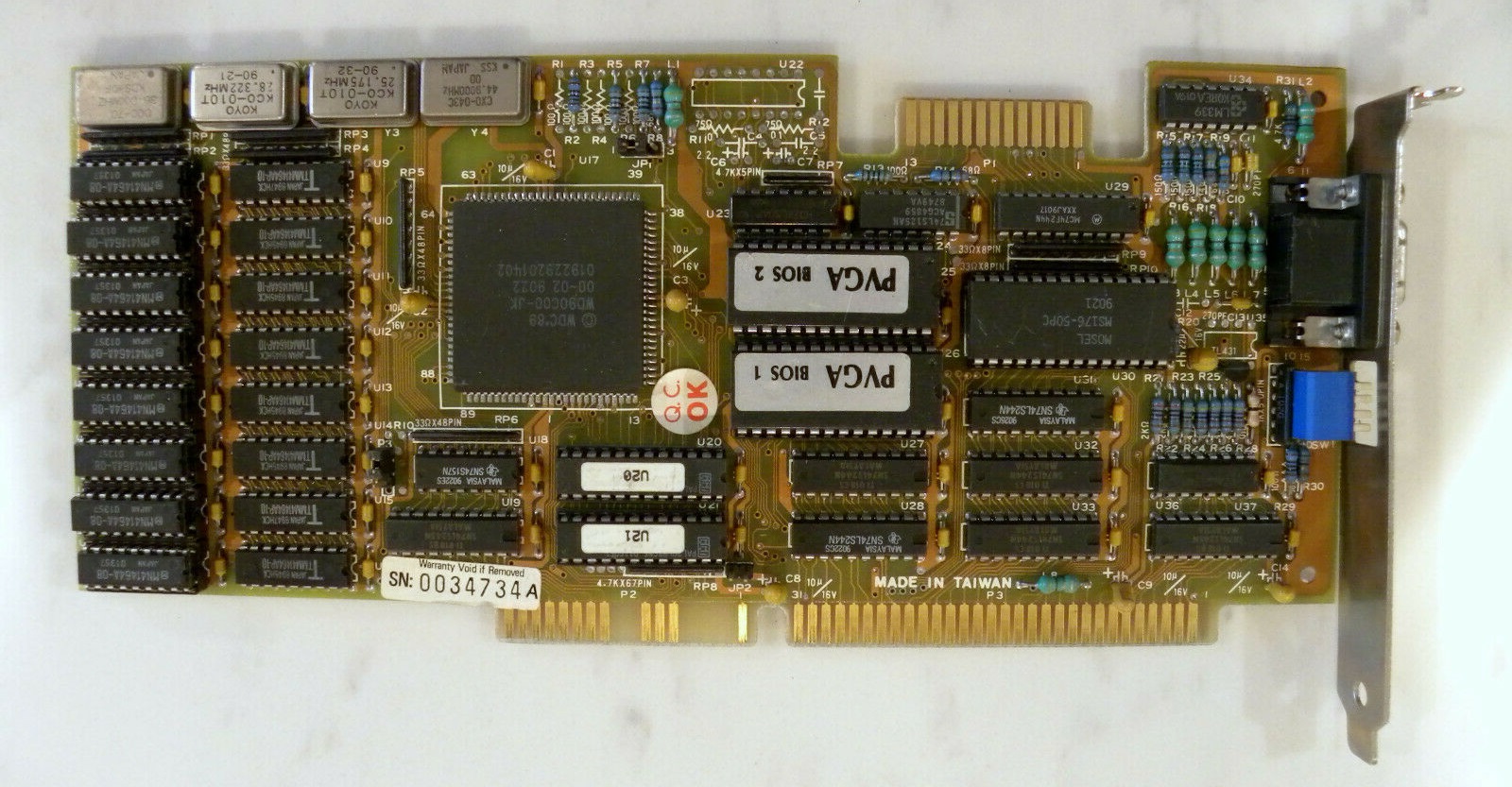
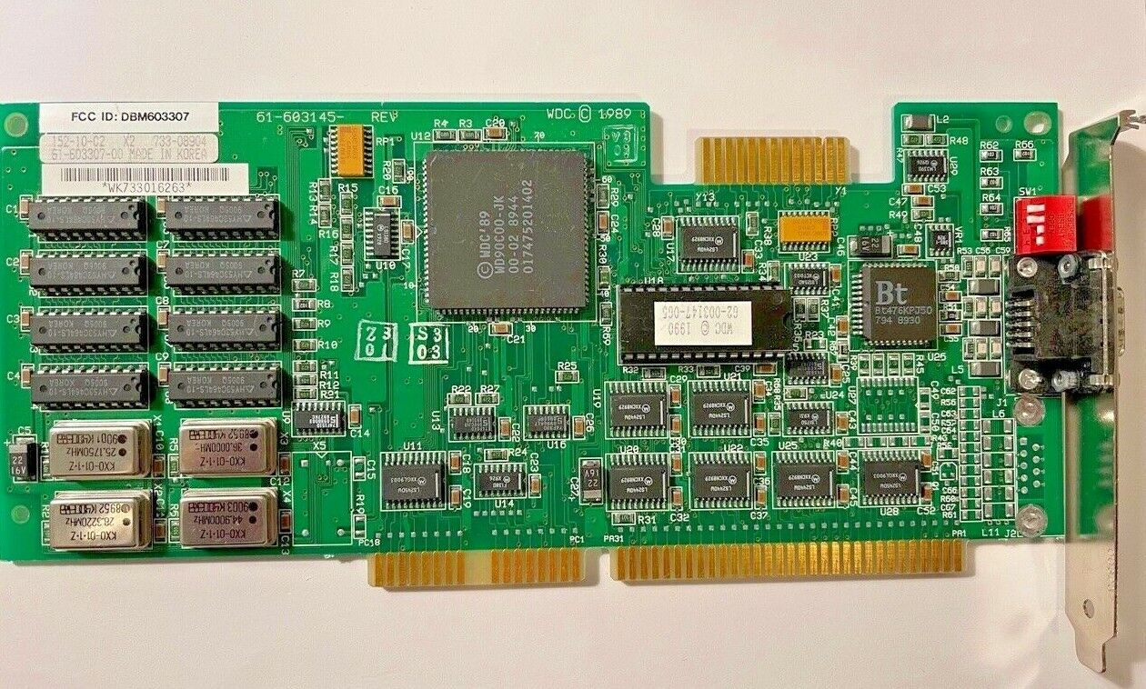
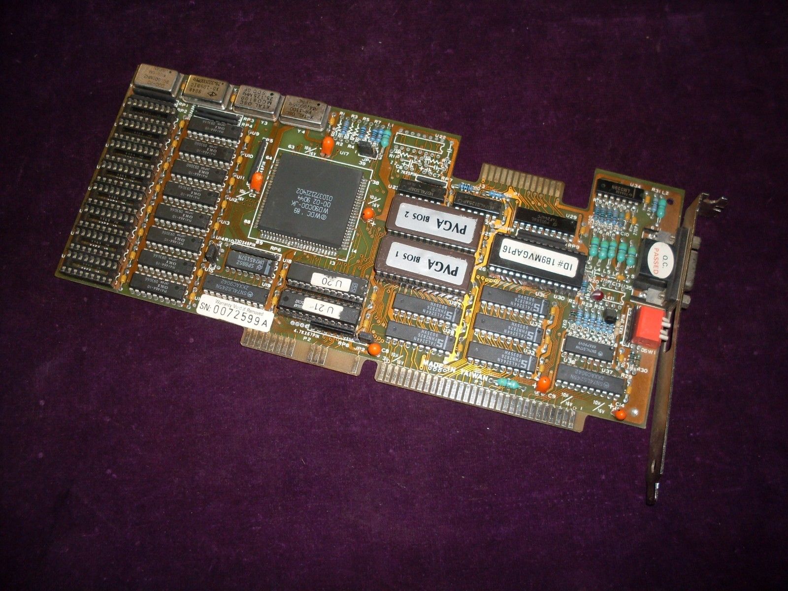
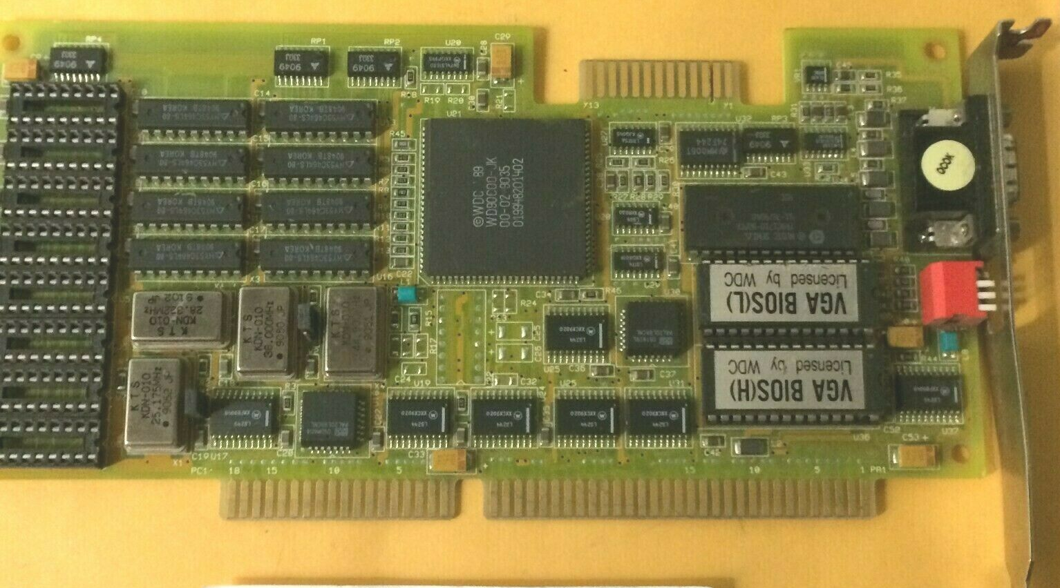
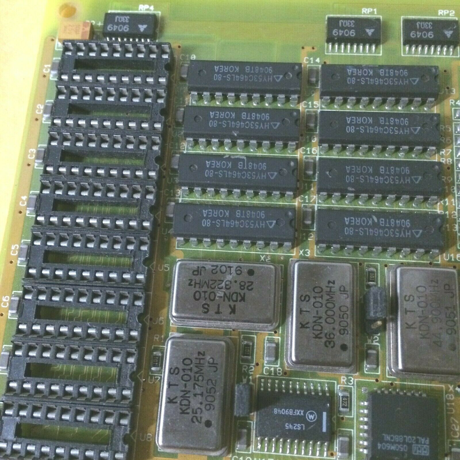
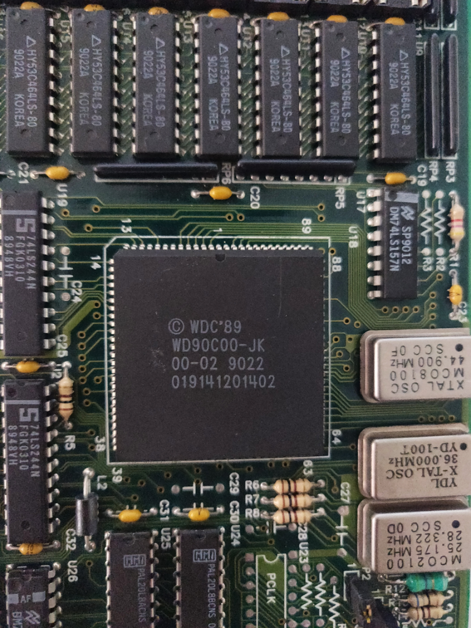
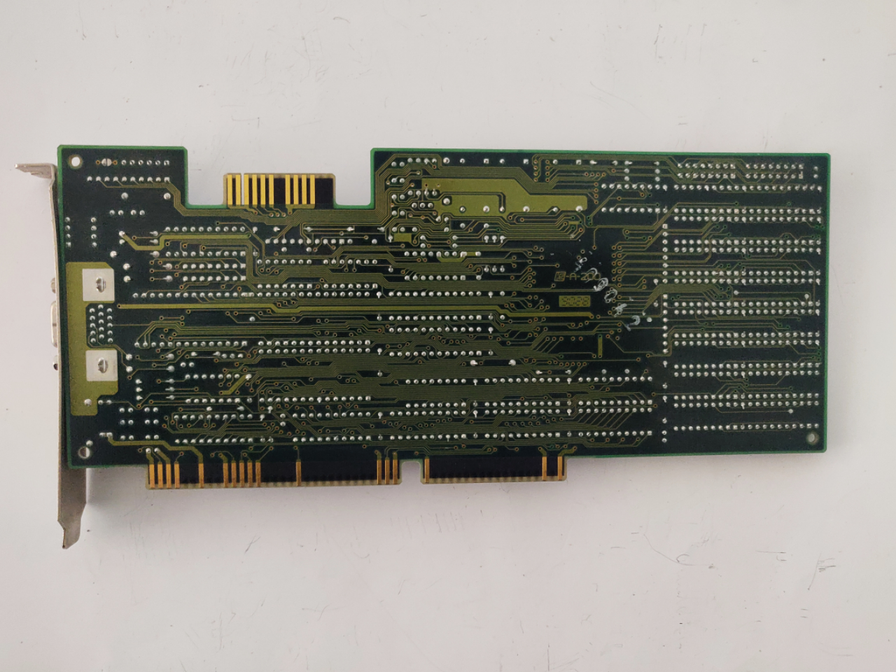
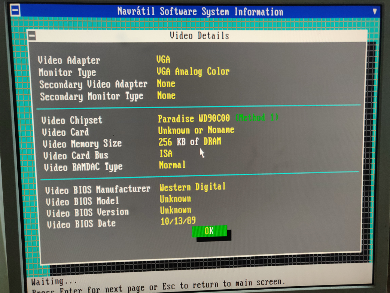
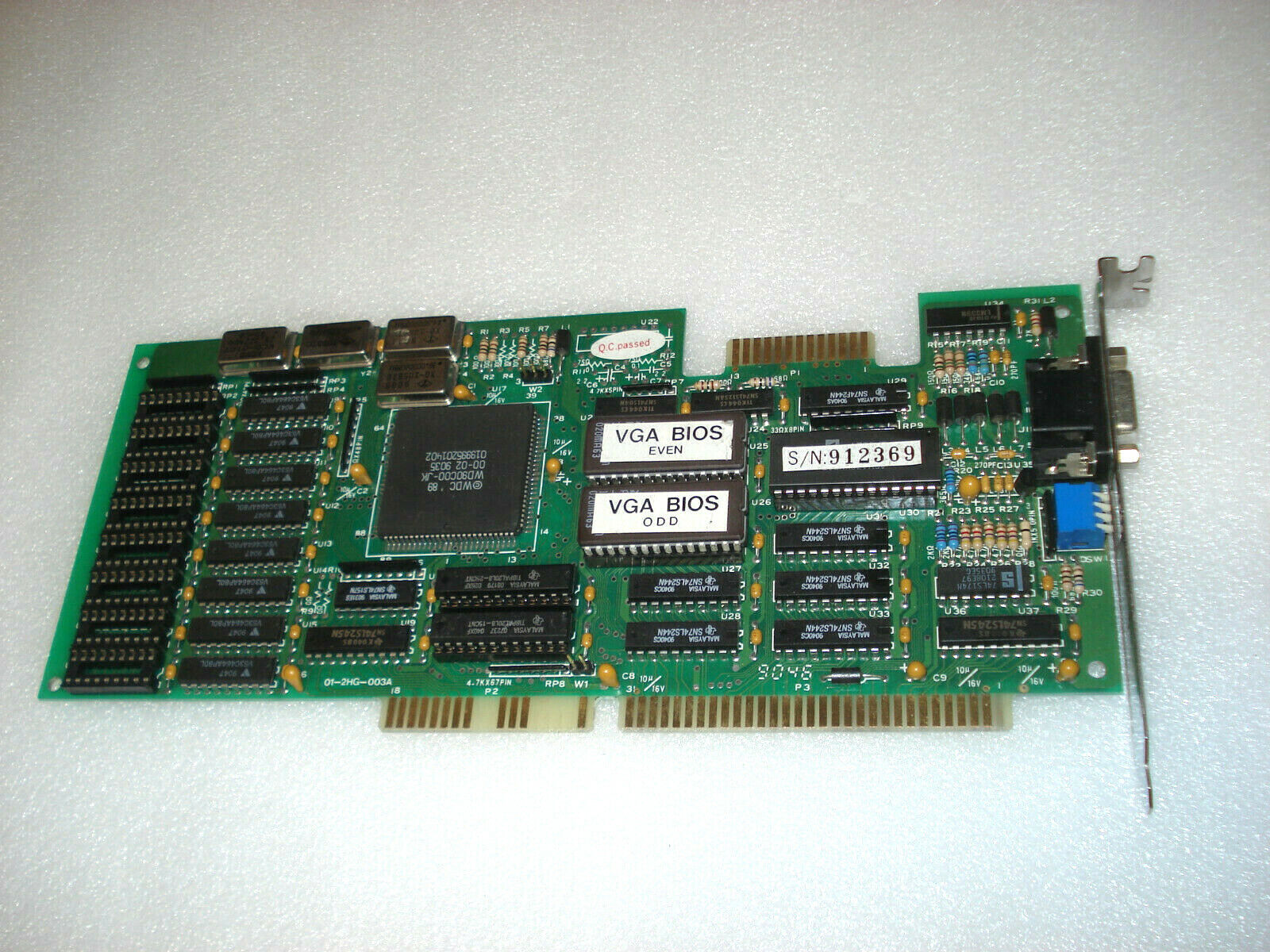
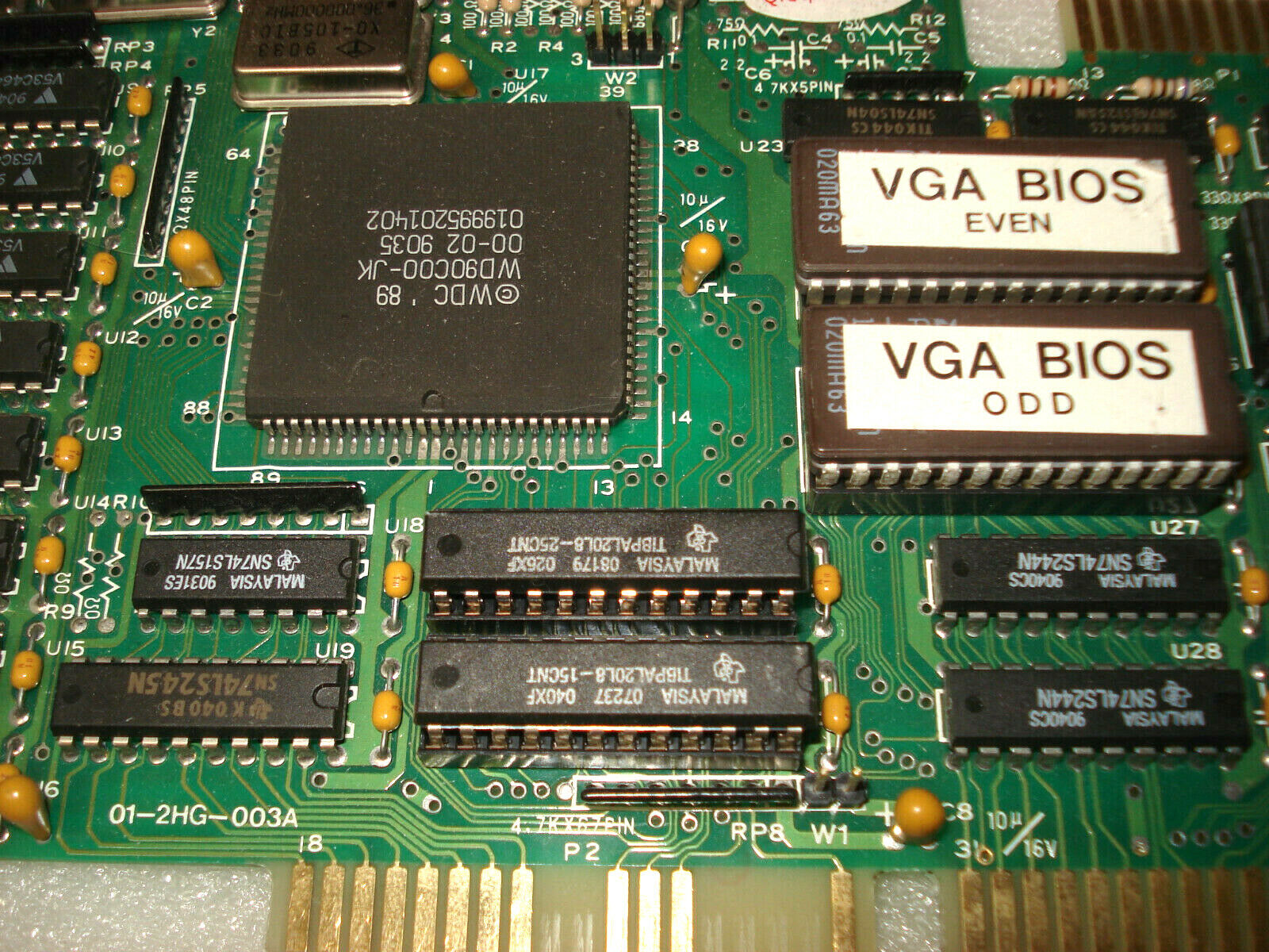
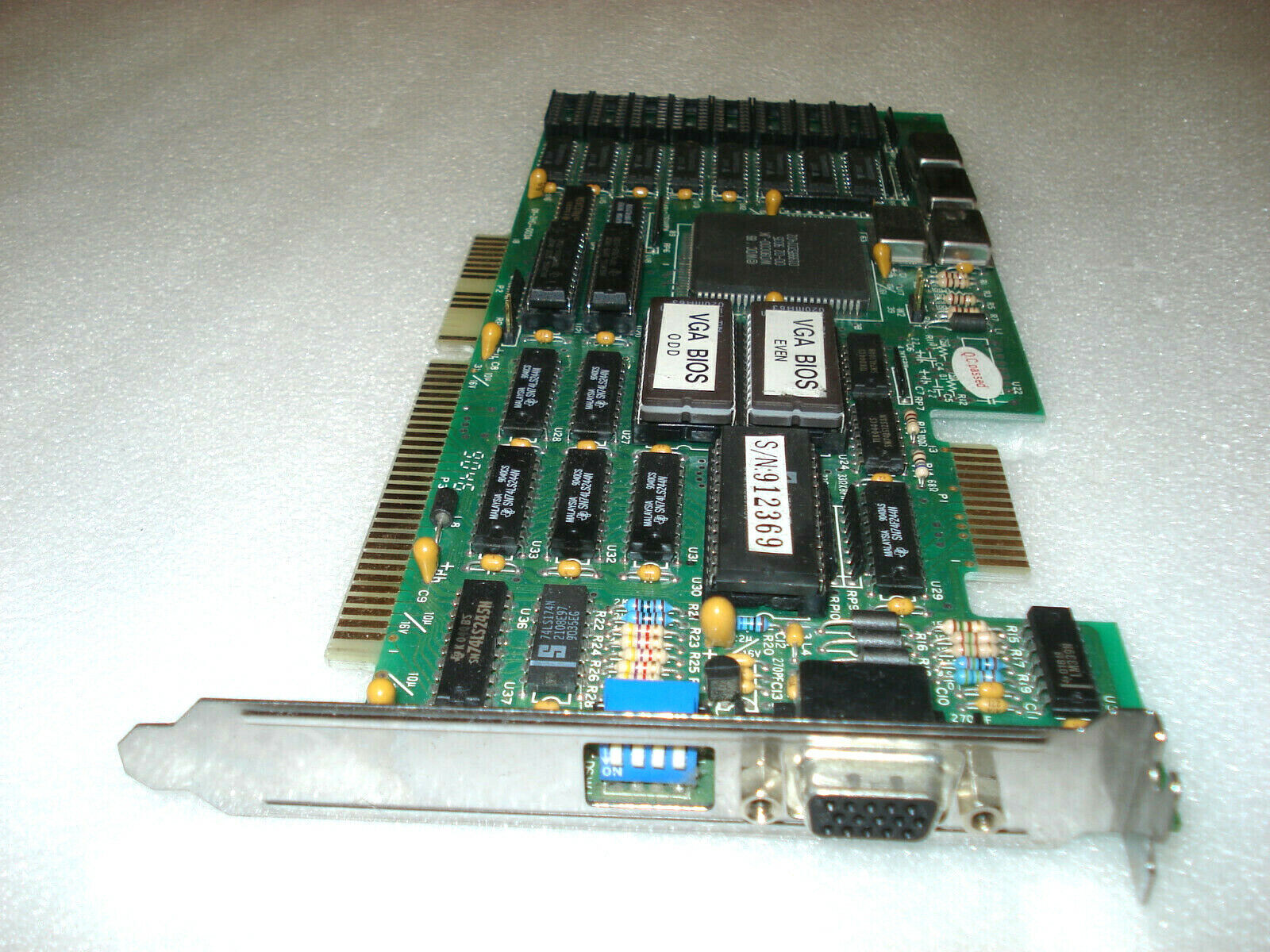
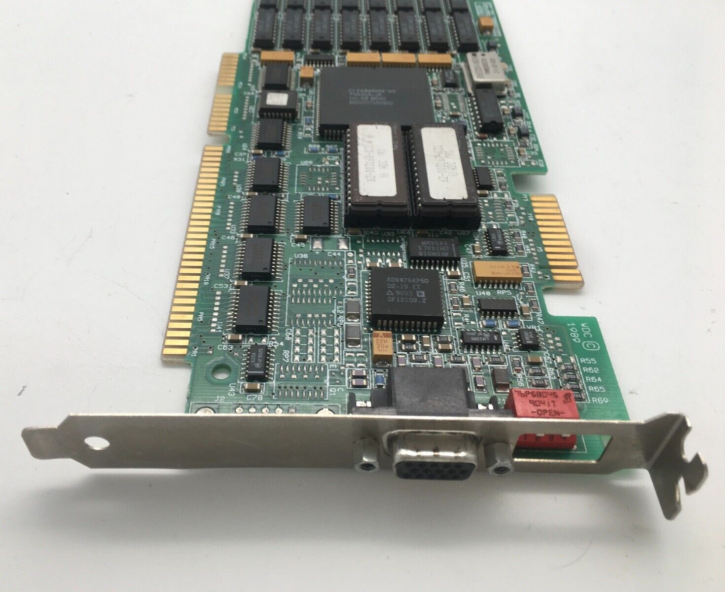
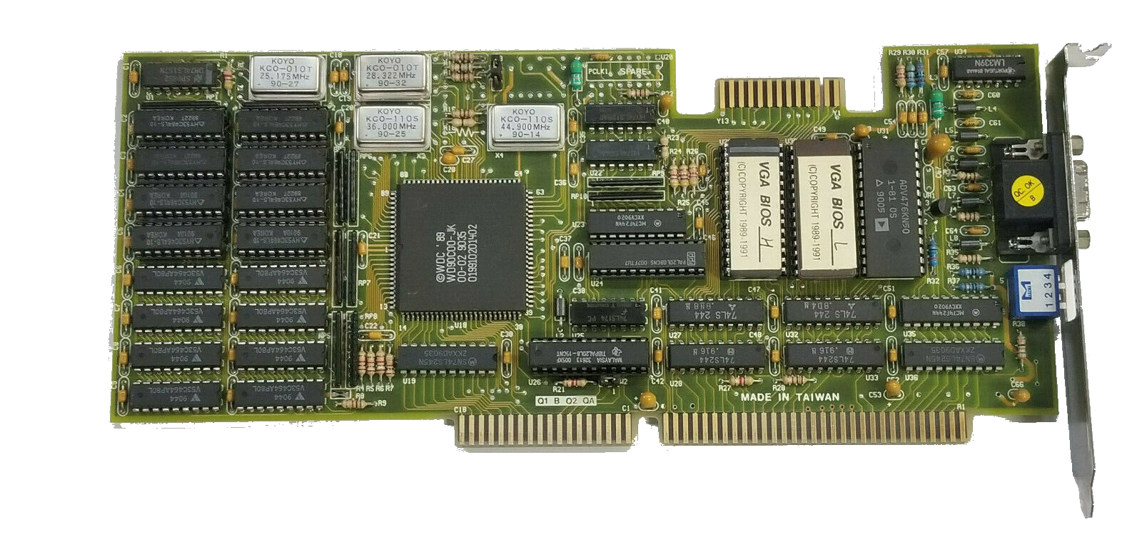 PVGA 1B (WD90C00)

Launched: 1989
Bus: ISA 16-bit
Memory: 256 KB, 512 KB or 1 MB (70, 80 or 100ns)
Core Clock: 45 MHz
Memory Speed: 56 MHz
RAMDAC: Analog Devices ADV476KN50 (8-bit colour depth, 256 colours), Brooktree Bt471KPJ66 or Brooktree Bt476KPJ50
RAMDAC Speed: 50 MHz or 66 MHz
VESA Standard: No, use UNIVBE or similar
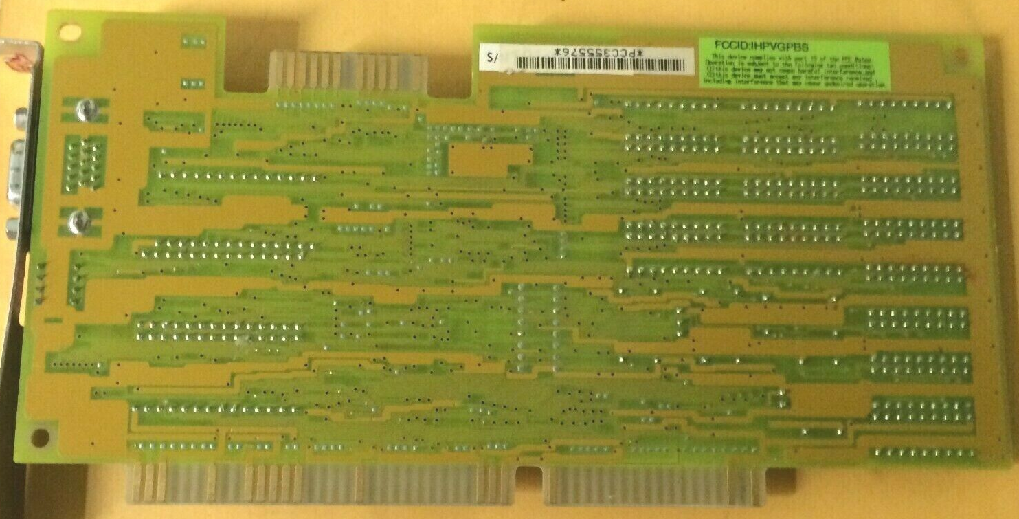
FCC ID: DBM603307 (Philips), DBM603316 (Philips), DBM603365 (Philips), IW9PVGA1024 (Datamatic System Co), IHPVGPVS (Brilliant Technology Co)
BIOS Dates: 10/13/89, 05/21/90
Known BIOS Versions: 003145-110
The WD90C00, originally called PVGA1B, is pin-compatible with the slightly earlier PVGA1A. It supports resolutions up to 1024 x 768 in 16 colours interlaced. It does support this resolution in a non-interlaced mode if an external 56 MHz clock and 80ns or faster DRAMs are installed on the card (a combination of video clock, memory clock, and DRAM speed determines the video modes that are available). It also supports up to 256 colours at 800 x 600 resolution.
Some cards based on the WD90C00 support 16 DRAMs while others have 8. Due to the way in which memory is organised, there are three memory configurations possible:
| Configuration | Total Memory | Maximum Resolution and Colours |
|---|---|---|
| Eight 64Kx4 DRAMs | 256 KB | 800 x 600 in 16 colours, or 640 x 400 in 256 colours |
| Sixteen 64Kx4 DRAMs | 512 KB | 1024 x 768 in 16 colours, or 640 x 480 in 256 colours |
| Eight 256Kx4 DRAMs | 1 MB | 1024 x 768 in 16 colours, or 800 x 600 in 256 colours |
So if you have only eight DRAM sockets on your card, it will not support 512 KB of video memory, only either 256 KB or 1 MB.
For my findings on the crystal oscillators on PVGA1B/WD90C00 cards, see the section at the bottom of this page called Paradise/WD Crystals.
Click here for the WD90C00 / PVGA1B datasheet.
WD90C00 and PVGA1B chips were used on the following cards:
- Philips unknown model (FCC ID: DBM603307)
- Philips unknown model (256 KB) (FCC ID: DBM603316)
- Philips unknown model (FCC ID: DBM603365)
- Philips VGA 16 (FCC ID: DBM5UEVGAPROF) - these cards can also be found with pin-compatible PVGA1A or WD90C90 instead.
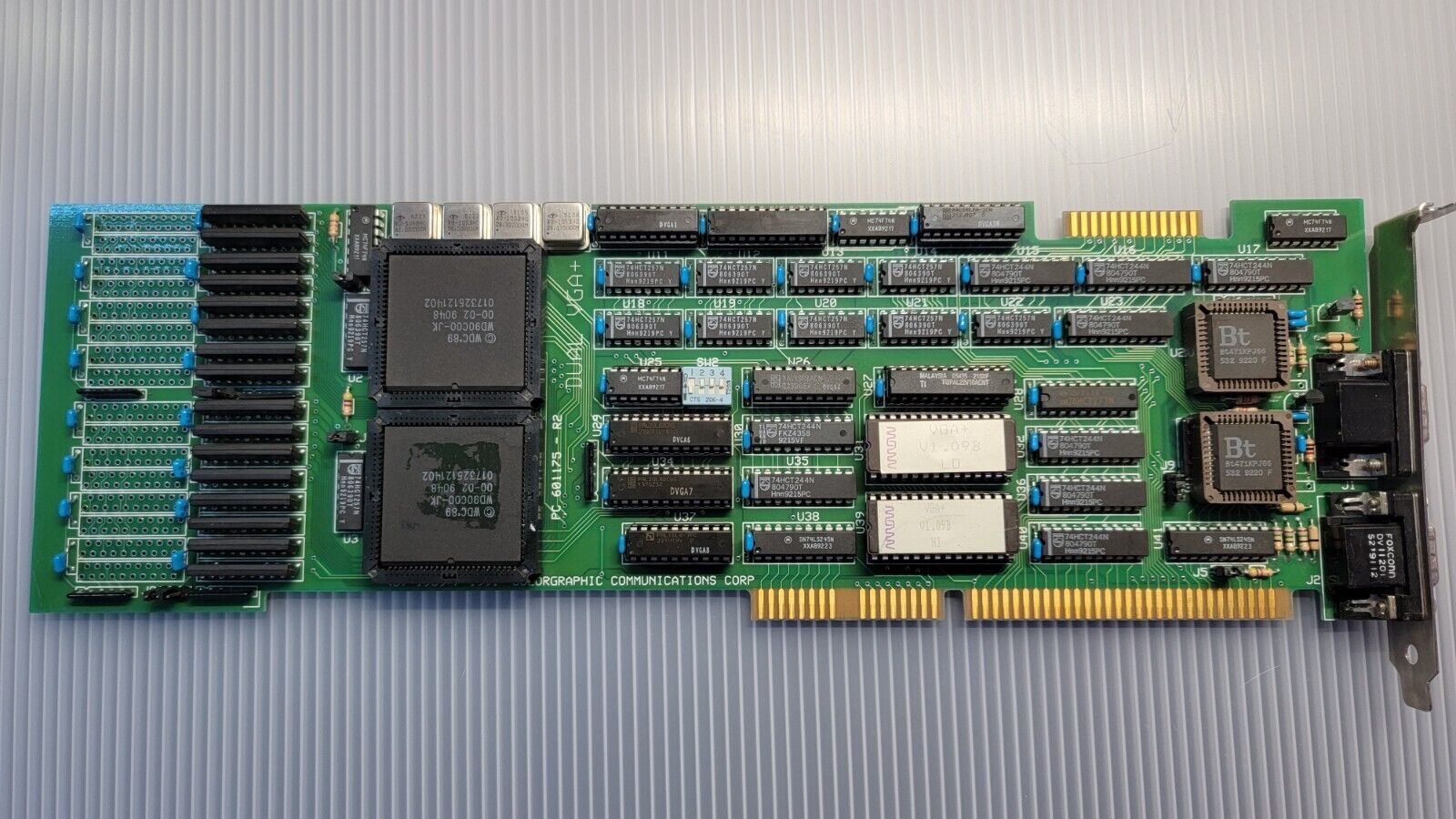
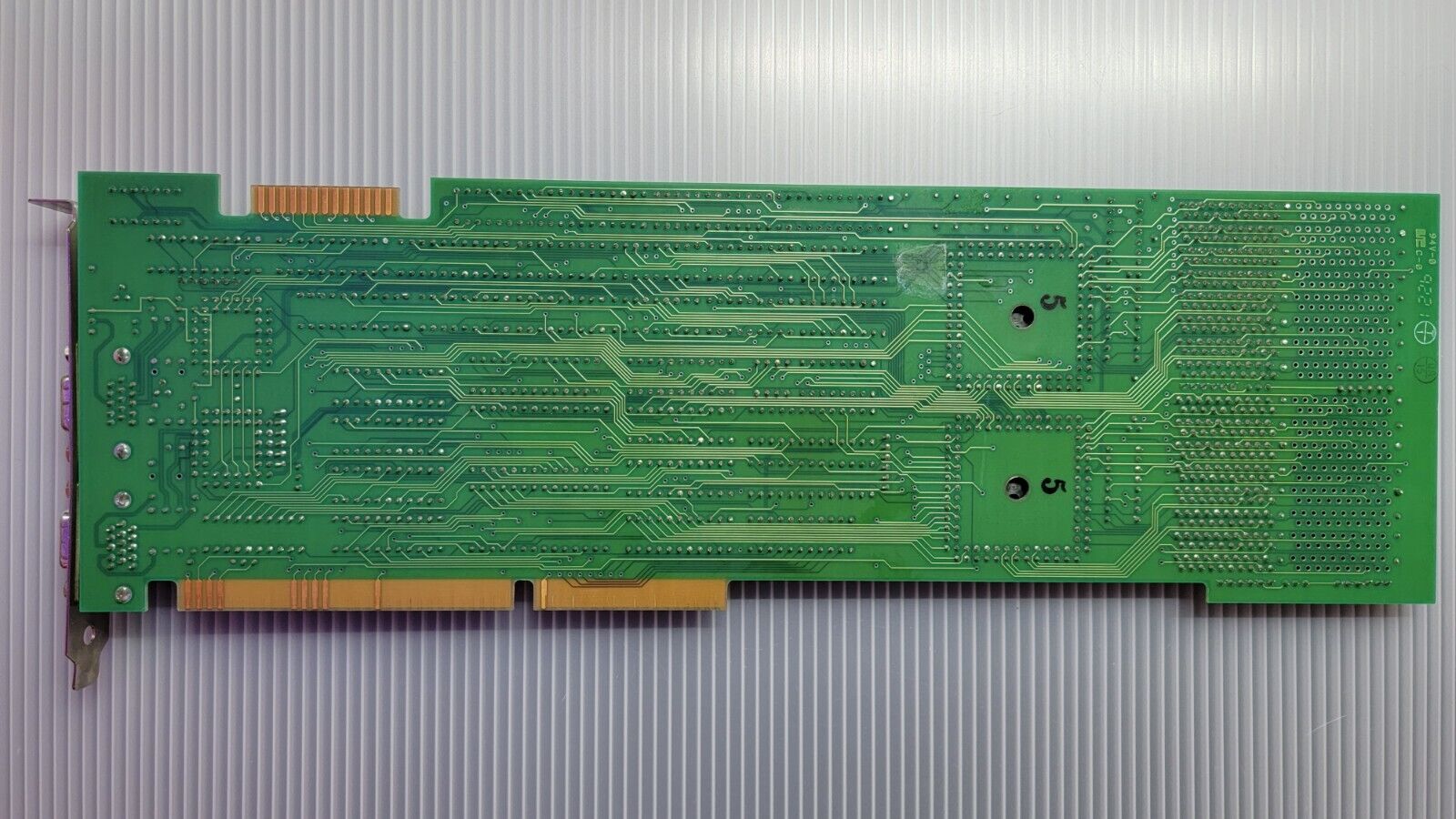
- Colorgraphic Communications Dual VGA+ (1991)
- Brilliant Technology Co. (FCC ID: IHPVGPVS)
- Datamatic System Co. (512KB) (FCC ID: IW9PVGA1024)
More Images
 PVGA 1M / WD90C10


Launched: 1989
Bus: ISA 16-bit
Memory: 256 KB (FPM DRAMs)
RAMDAC: 42 MHz
Supports resolutions up to 1,024 x 768 in 4 colours or 800 x 600 in 16 colours. 65 MHz core clock and 42 MHz memory clock. Up to 256 KB display memory supported (70ns or 80ns).
Click here for the WD90C10 Datasheet
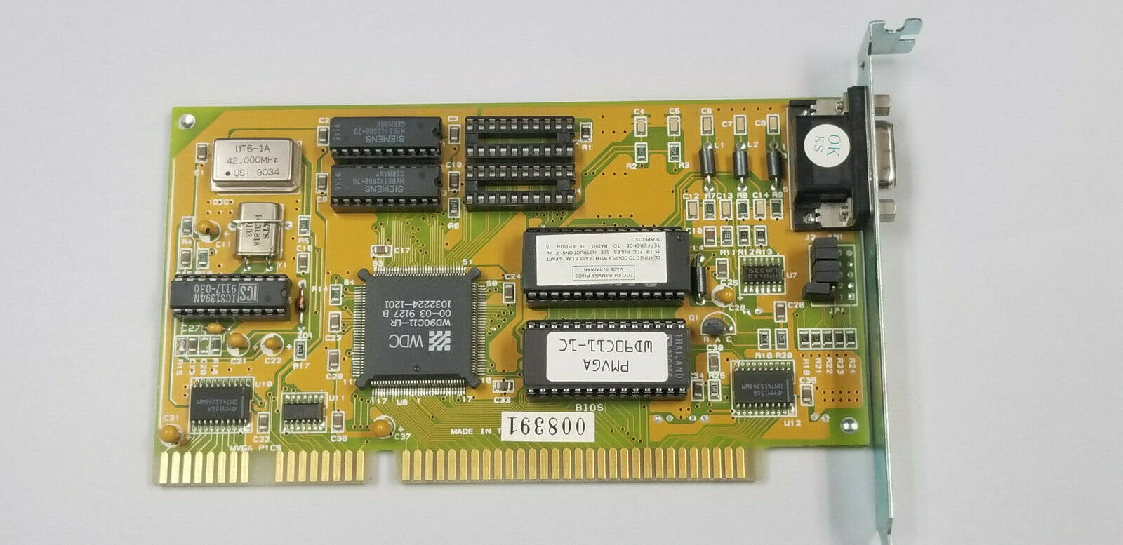
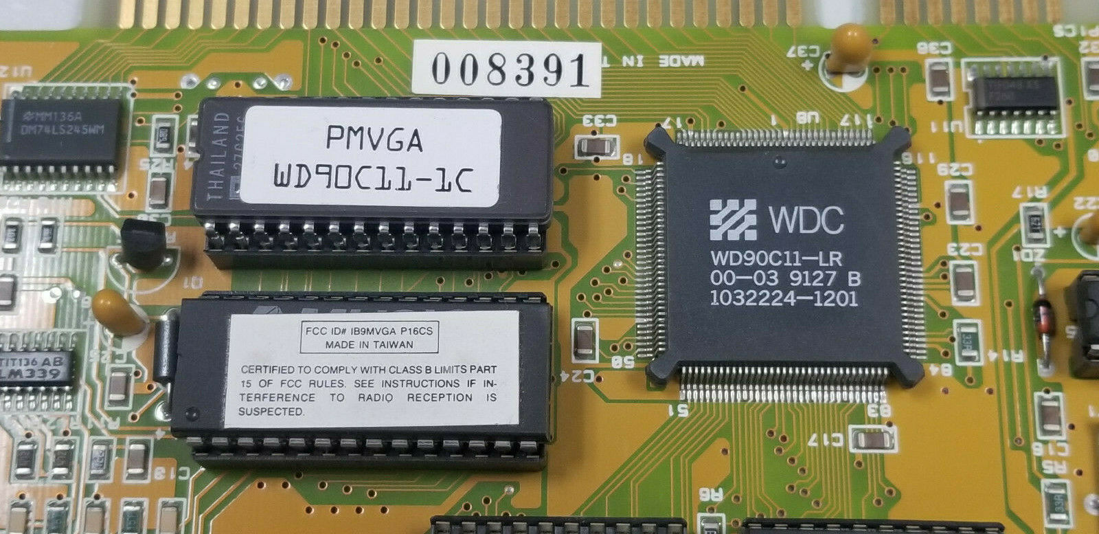
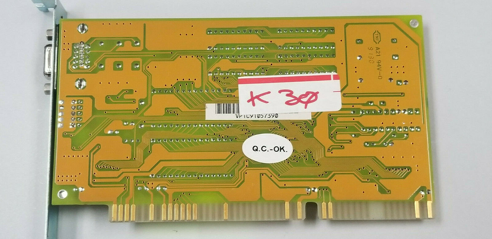
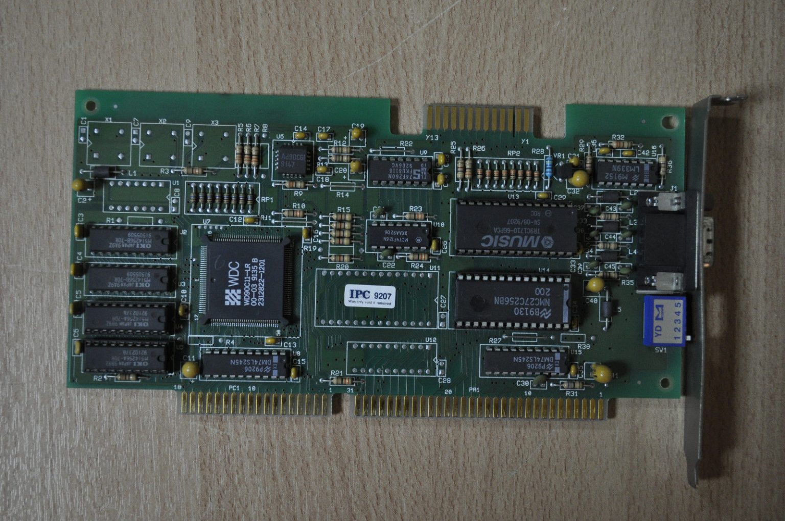
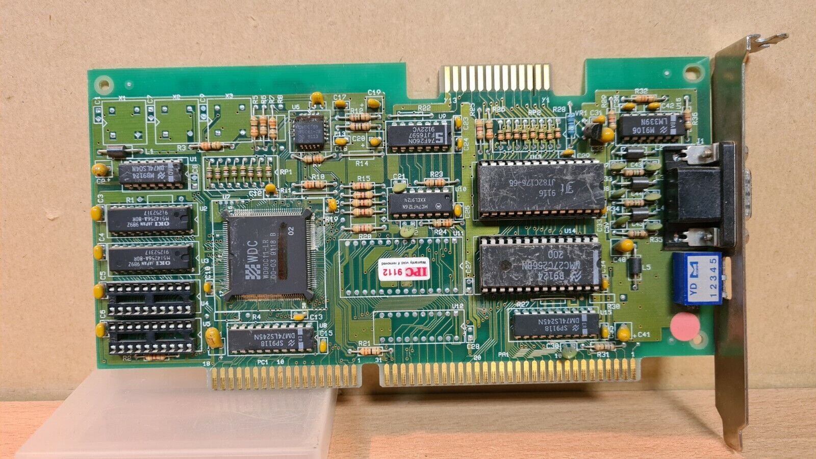
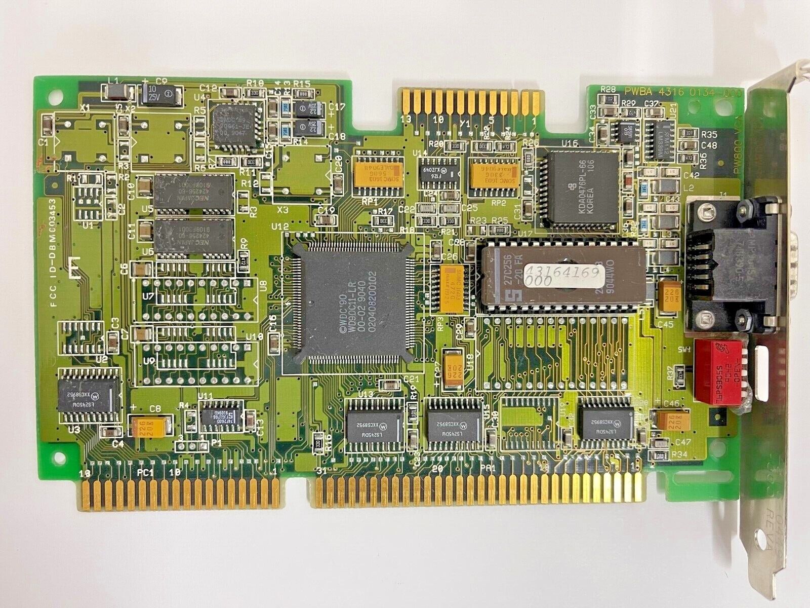
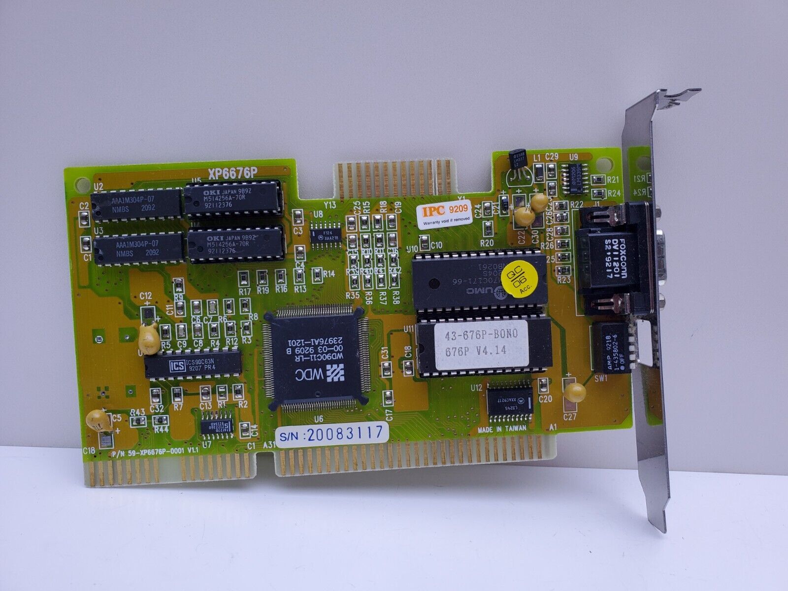
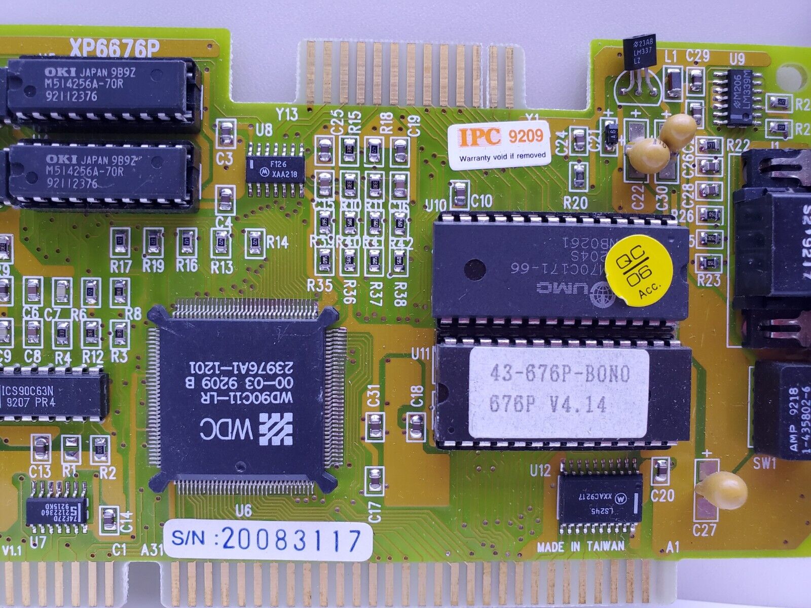
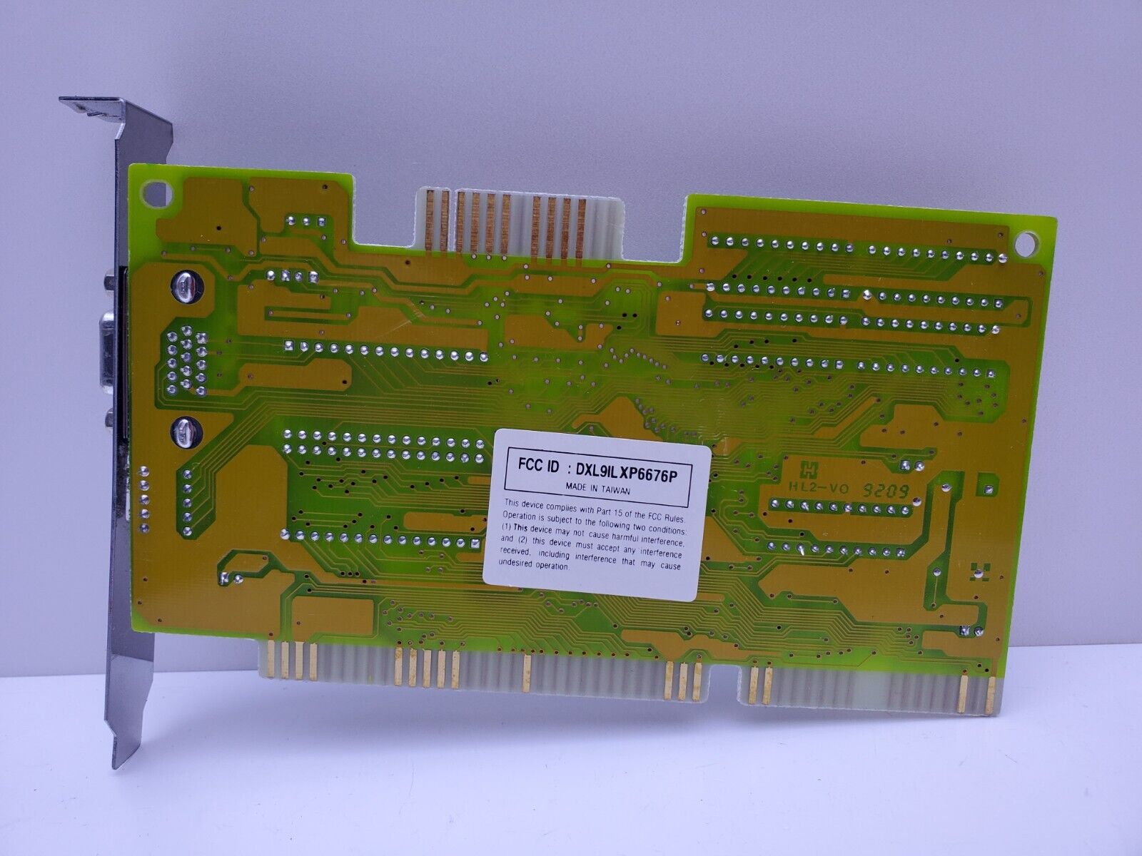
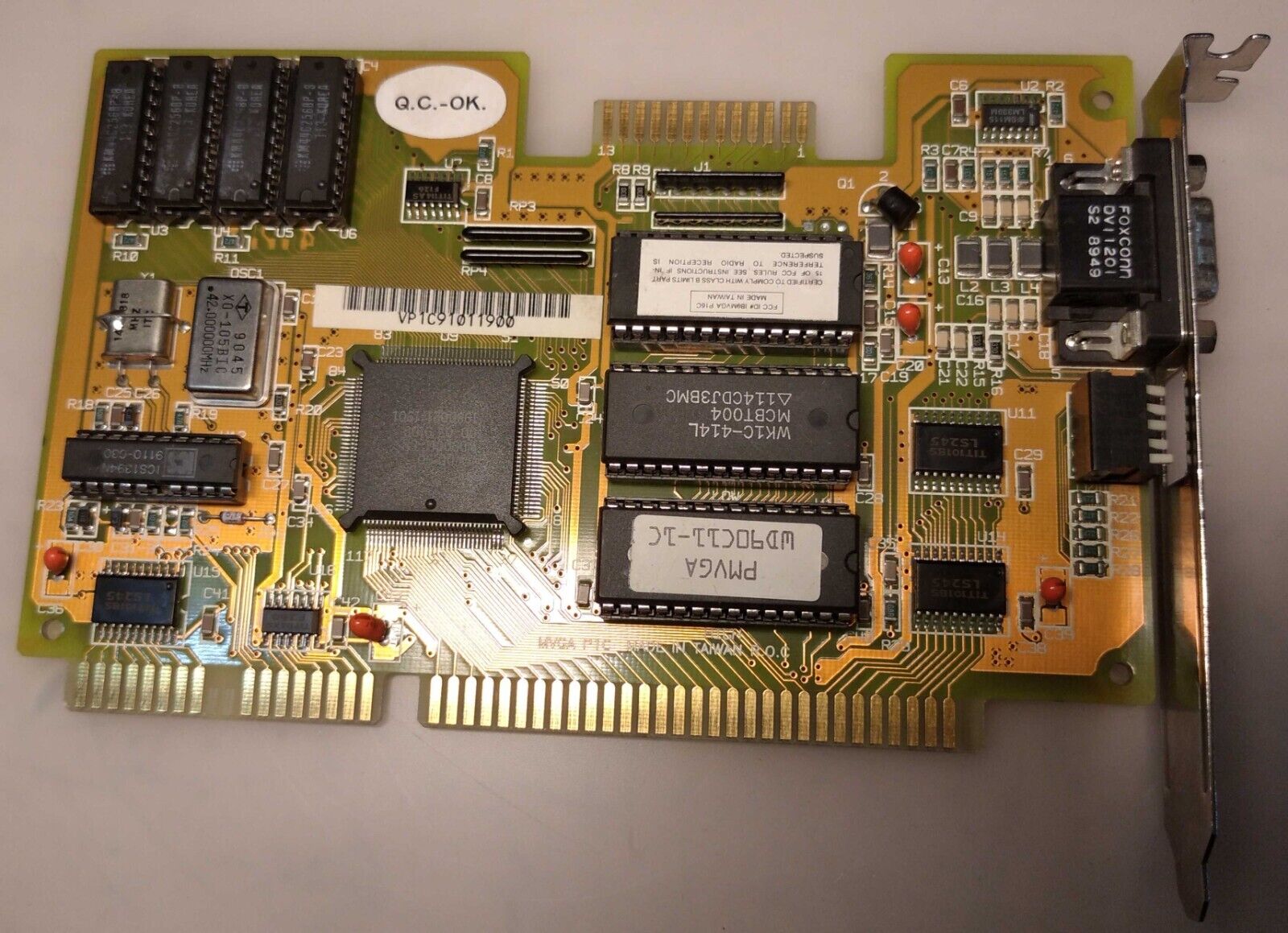
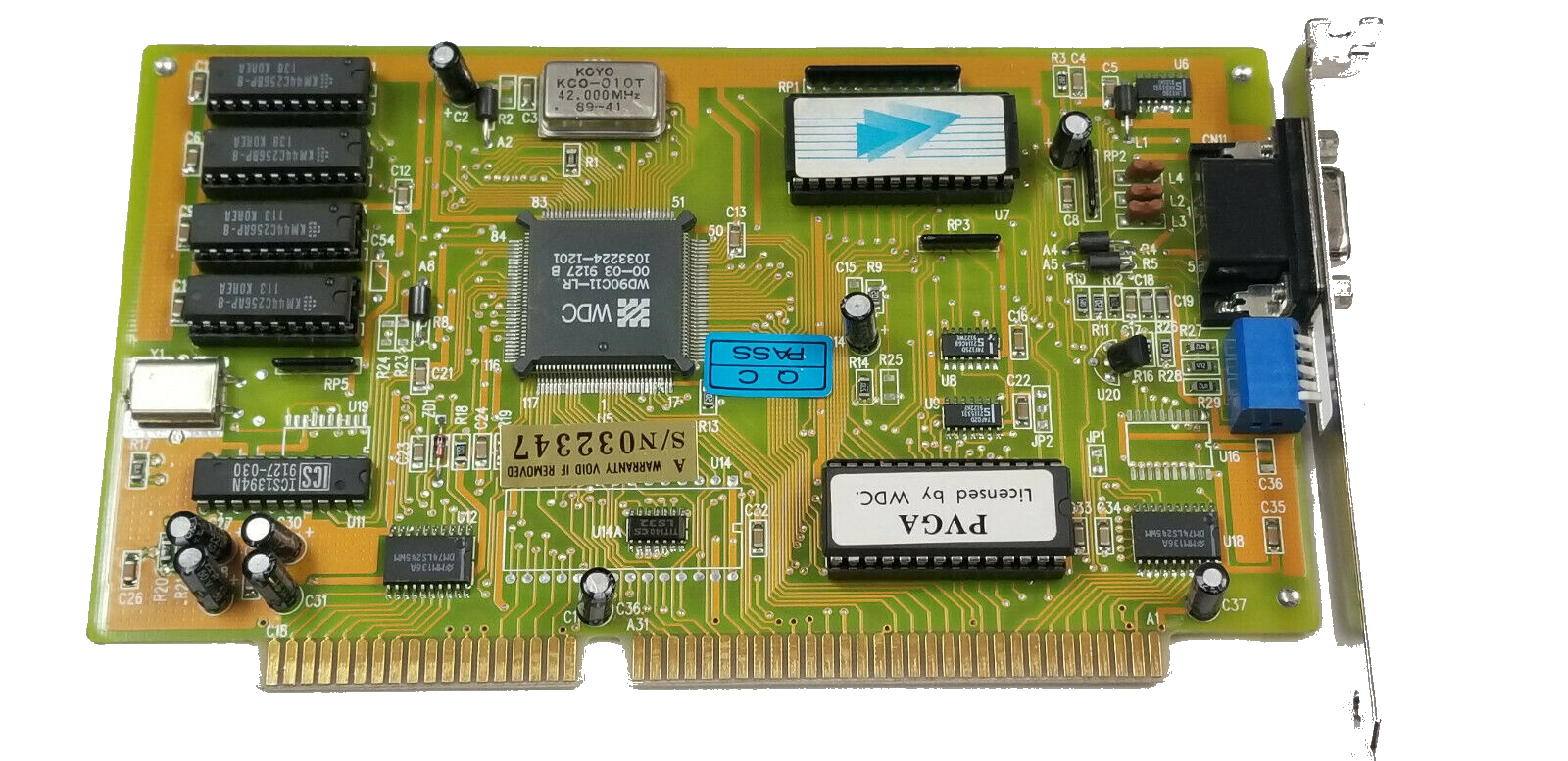 WD90C11 / WD90C11A


Launched: 1989
Bus: ISA 16-bit
Memory: 256 KB or 512 KB (FPM DRAMs)
RAMDAC: Music Semiconductor TR9C1710 or Samsung KDA0476PL
RAMDAC Speed: 45 MHz
VESA Standard: Yes, v1.0
FCC ID: DBMC03453, DX9ILXP6676P
BIOS Dates: 12/13/90
Known BIOS Versions:
An "Enhanced VGA controller" from Western Digital - the WD90C11-LR chipset. The WD90C11 used a 1.25 micron process, and WD90C11A used the later 0.9 micron process for manufacture. Highlights of the chipset include:
- On 512 KB video RAM boards, resolutions up to 1024 x 768 in 16 colours interlaced or non-interlaced (plus 640 x 400, 640 x 480, 800 x 600, all in 256 colours)
- On 256 KB video RAM boards, resolutions up to 1024 x 768 in 2/4 colours, or 800 x 600 in 16 colours
- 132-column text mode and 6-9 pixels wide fonts
- Integrated CRT controller, sequencer, graphics controller and attribute controller
- Write cache for improved CPU write performance
- 8- or 16-bit data bus for I/O and memory. True 16-bit CPU-to-video memory transfer for all modes
- Up to 65 MHz maximum video clock rate
- Up to 42 MHz maximum memory clock rate (90C11) or 45 MHz (90C11A)
- Supports all VGA modes if using two 64Kx16 DRAMs
- Full VGA hardware and BIOS compatibility
- EGA register-level compatibility on analog, TTL, and multi-frequency monitors
- Backward compatibility with MDA, CGA, EGA, Hercules and AT&T 6300
- Flexible RAM options, including two 256Kx4 DRAMs (256 KB of video RAM), or four 256Kx4 DRAMs (512 KB of video RAM)
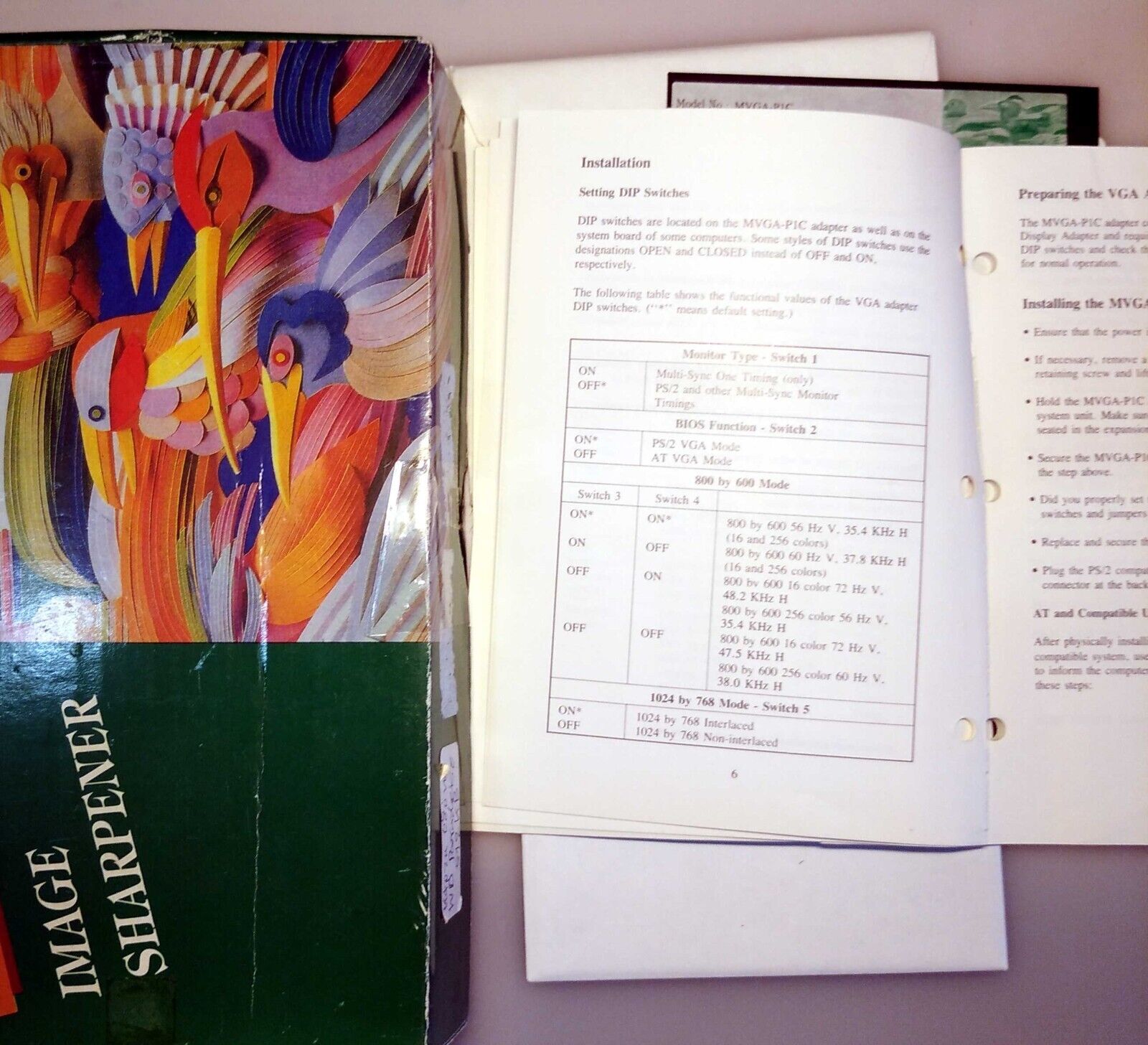
The five DIP switches normally found on WD90C11-based cards have these meanings:
| DIP Switch | Settings |
|---|---|
| 1 | Monitor Type: ON = Multi-Sync One timing (only) OFF = PS/2 and other Multi-Sync monitor timings |
| 2 | BIOS Function: (unsure what this does - perhaps changes the memory location of the VGA BIOS extensions or is related to ISA vs MCA architecture) ON = PS/2 VGA mode OFF = AT VGA mode |
| 3 and 4 | 800 x 600 Mode: ON ON = 800 x 600, 56 Hz refresh rate, 35.4 KHz horiz. sync (16 and 256 colours) ON OFF = 800 x 600, 60 Hz refresh rate, 37.8 KHz horiz. sync (16 and 256 colours) OFF ON = 800 x 600, 72 Hz refresh rate, 48.2 KHz horiz. sync (16 colours) *or* 800 x 600, 56 Hz refresh rate, 35.4 KHz horiz. sync (256 colours) OFF OFF = 800 x 600, 72 Hz refresh rate, 47.5 KHz horiz. sync (16 colours) *or* 800 x 600, 60 Hz refresh rate, 38.0 KHz horiz. sync (256 colours) |
| 5 | 1024 x 768 Mode: ON = Interlaced OFF = Non-interlaced |
Click here for the WD90C11 datasheet.
The WD90C11 and WD90C11A can be found on the following cards:
- Octek PVGA1C
- Phillips PW800 VGA (FCC ID: DBM003453)
- Unknown card (FCC ID: IB9MVGA P16CS)
- Lung Hwa Electronics XP6676P (FCC ID: DXL9ILXP6676P)
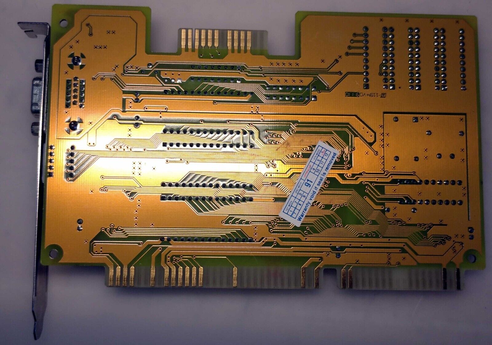
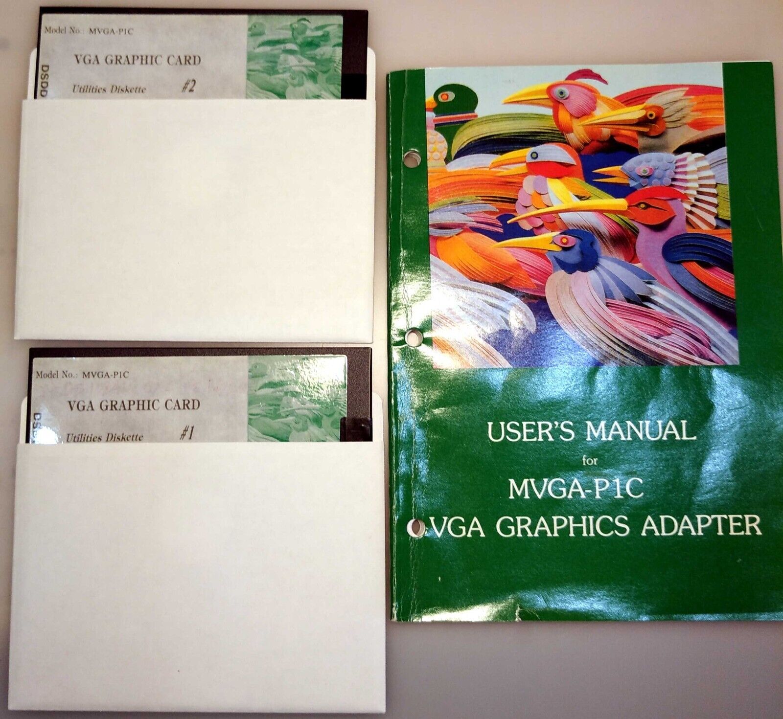
- HITA (Higher Intellect Technology) MVGA-P1C
More Images
WD90C12
Launched: 1990
Bus: ISA 16-bit
Memory: 256 KB or 128 KB (FPM DRAMs)
RAMDAC: ?
No further information is known on the WD90C12.
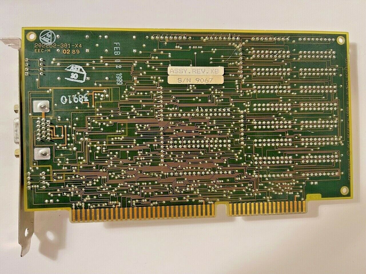
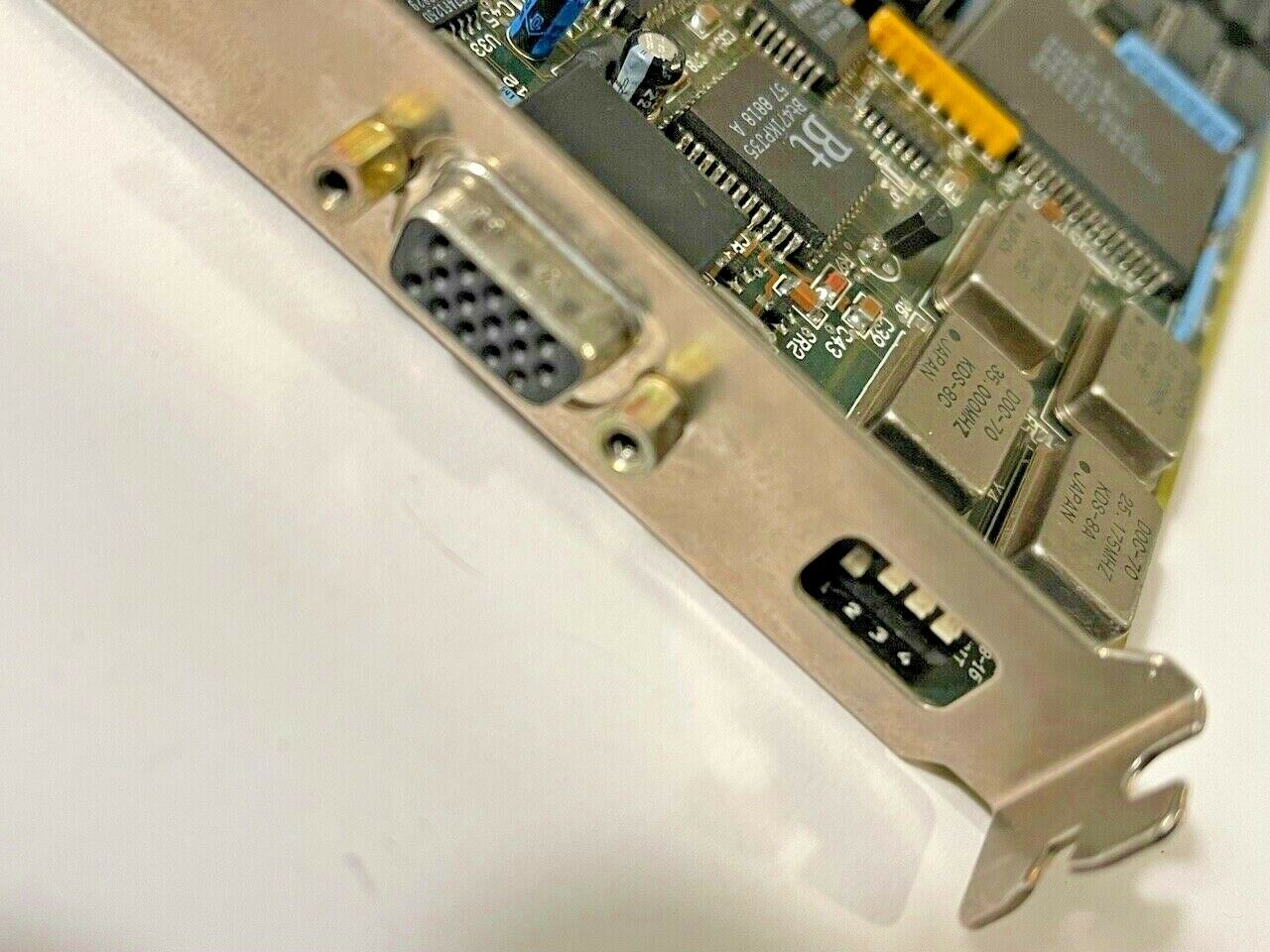
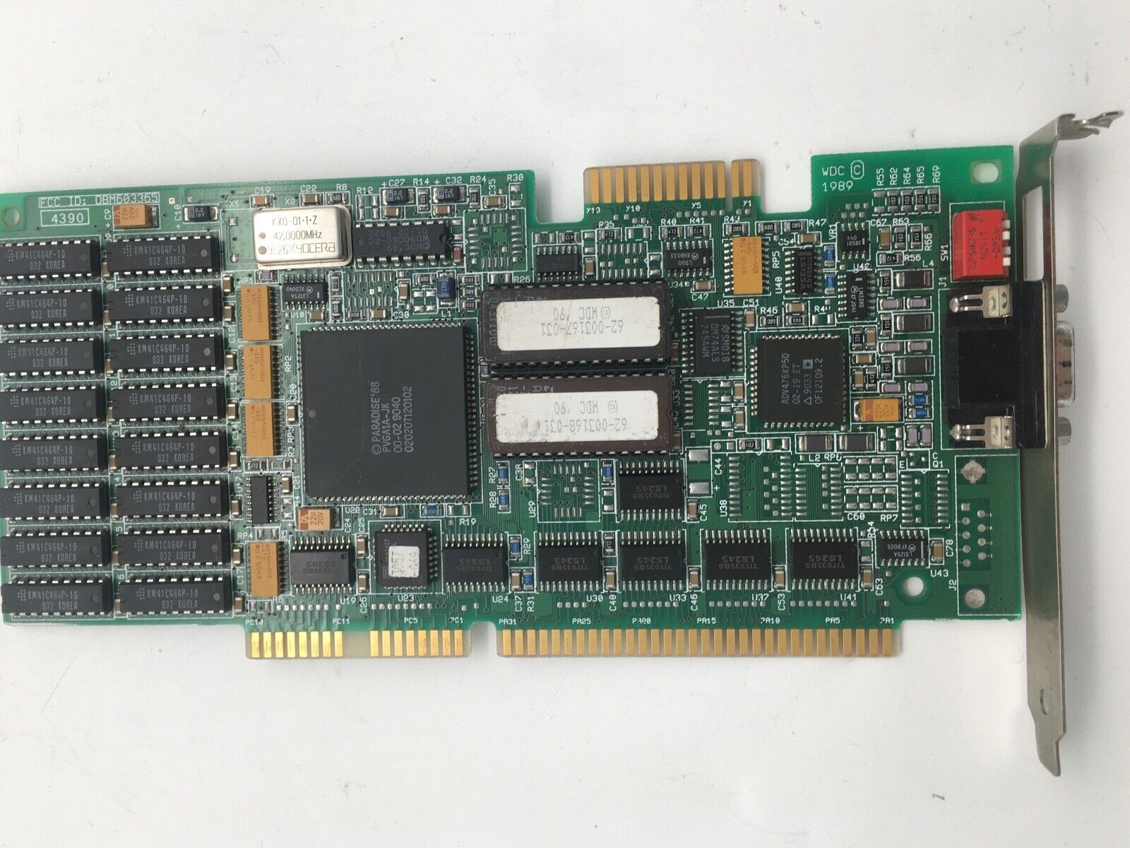
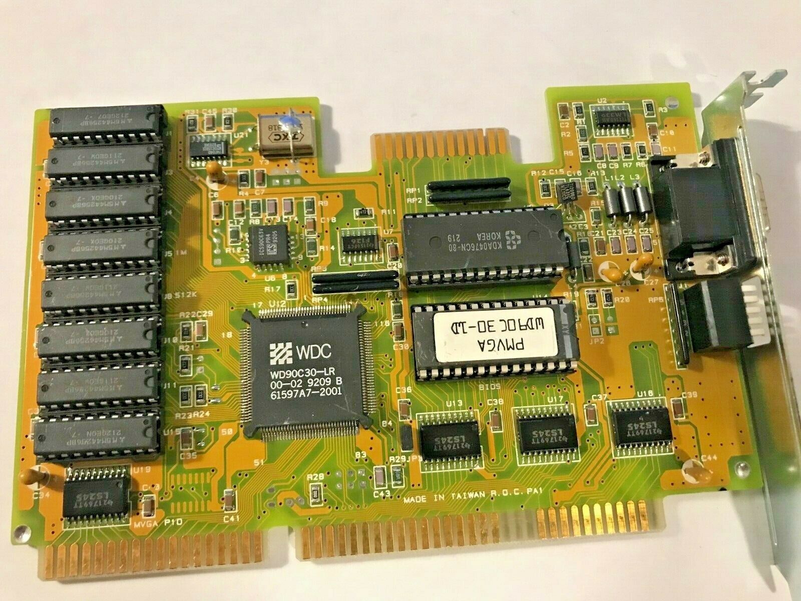
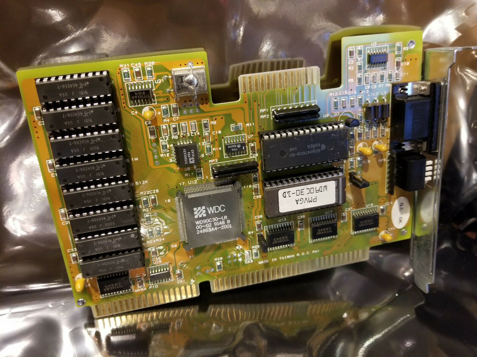
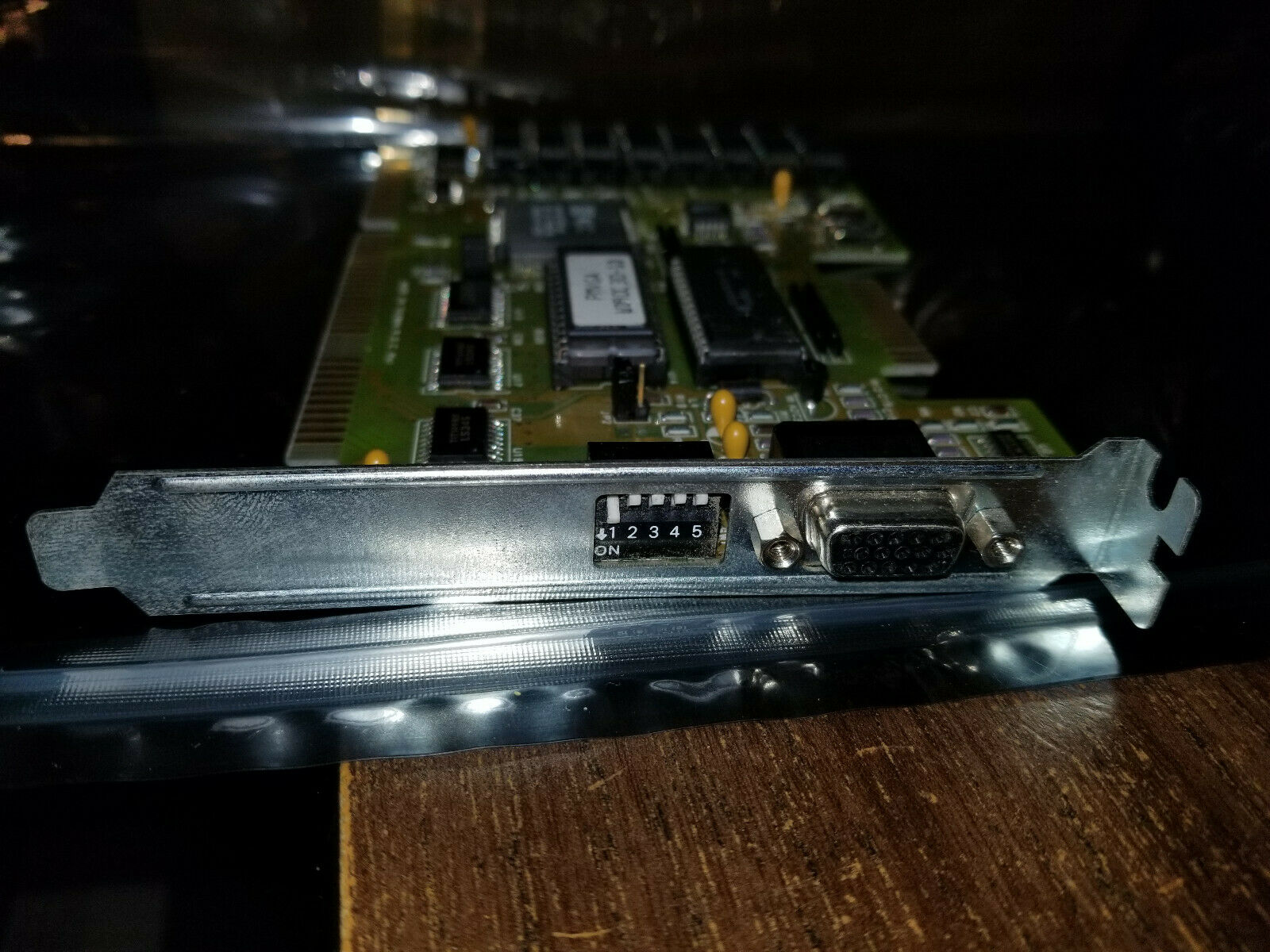
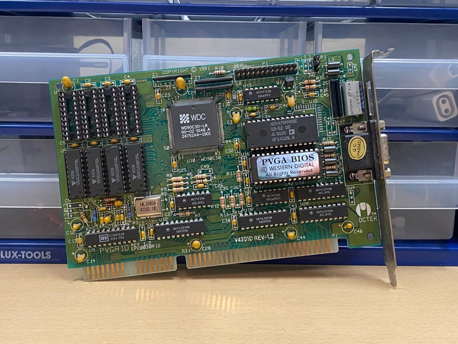
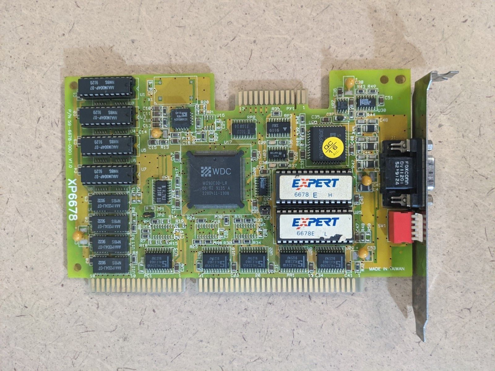
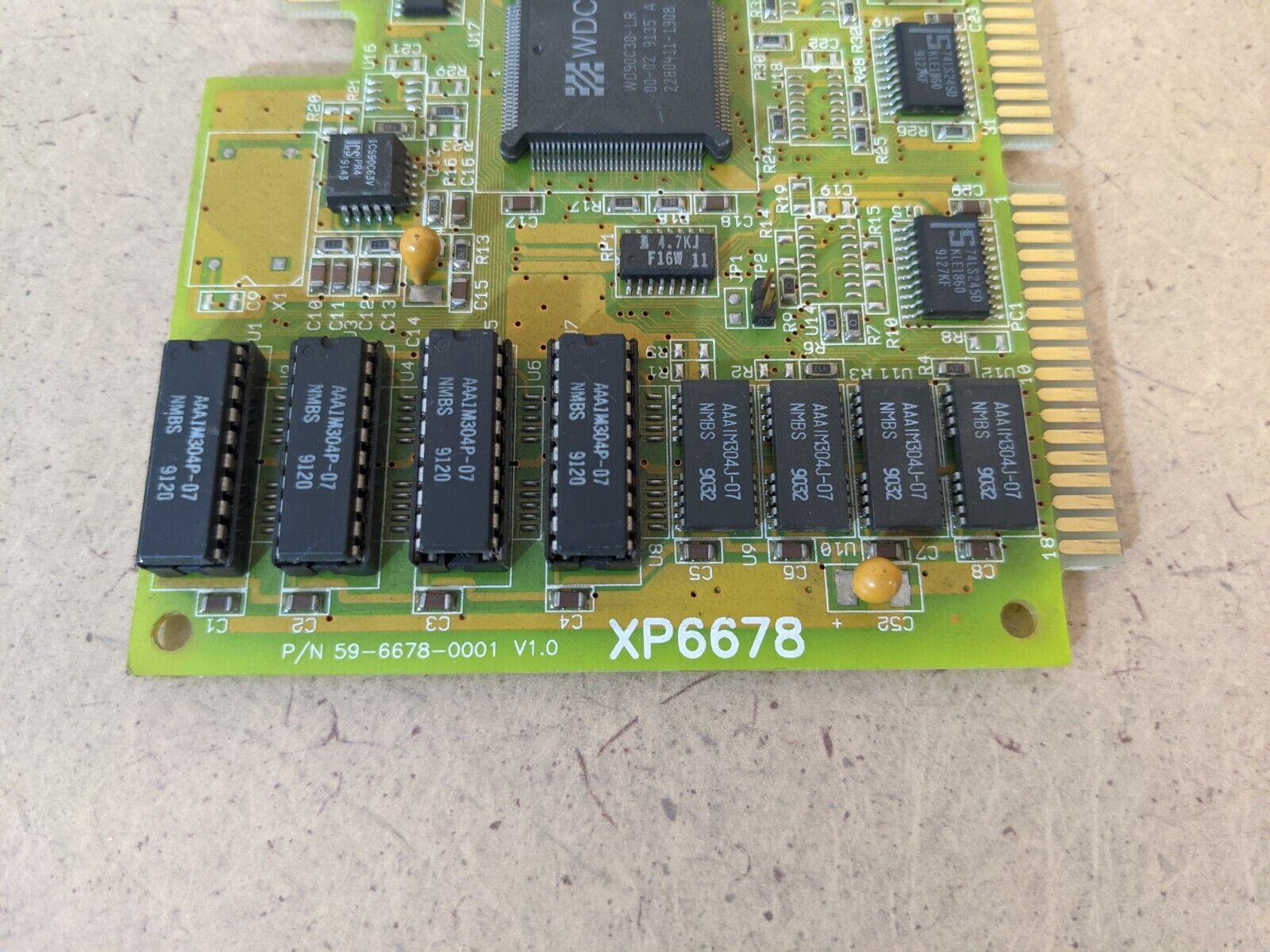
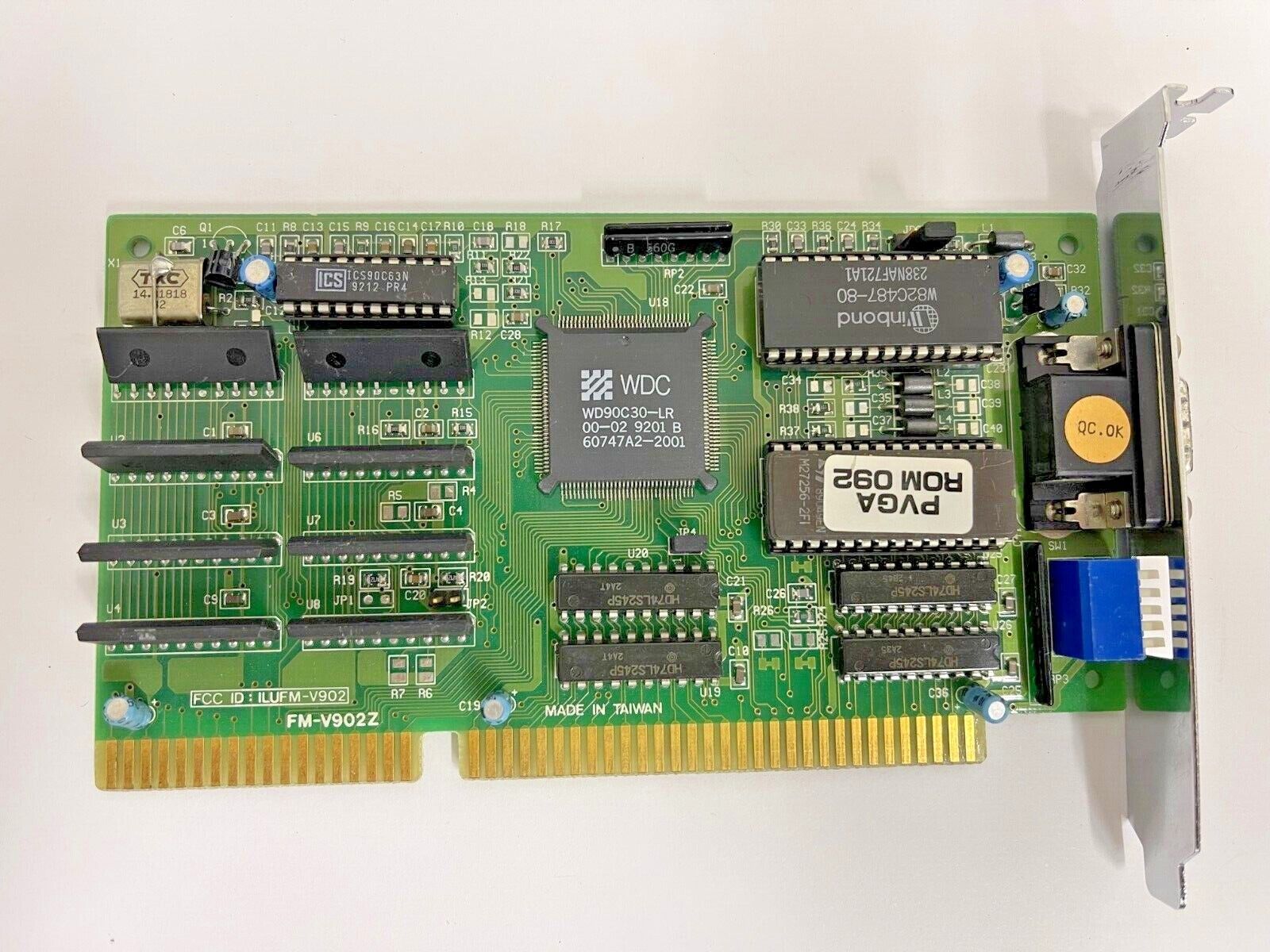
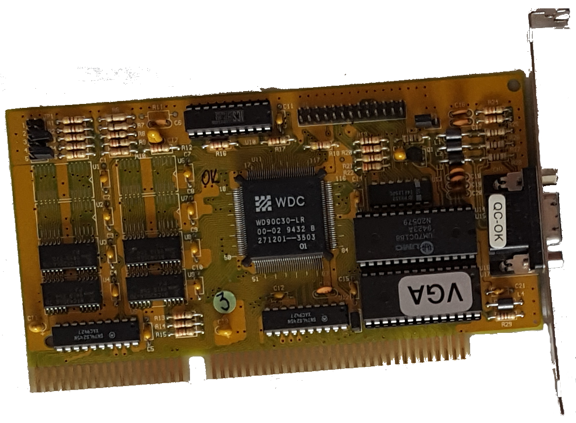 WD90C30
Launched: 1990
Bus: ISA 16-bit
Memory: 512 KB or 1 MB
Chipset: Western Digital WD90C30
RAMDAC: HiColor?
RAMDAC Speed: Up to 80 MHz
VESA Standard: 1.01
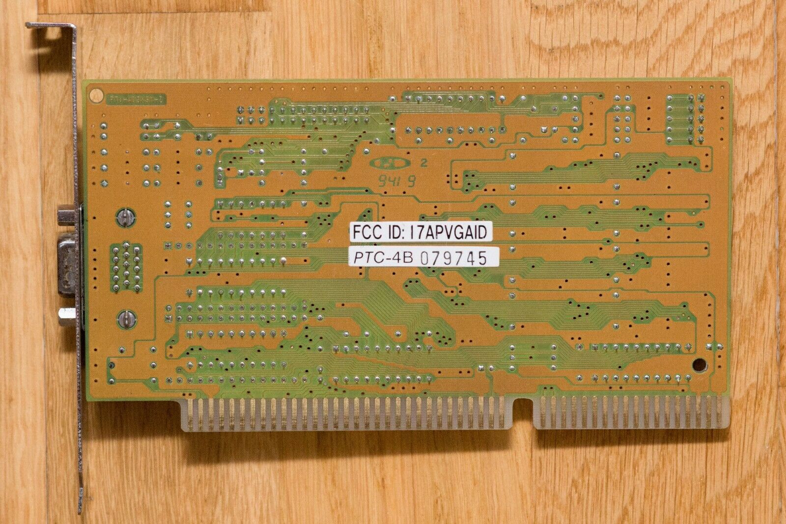
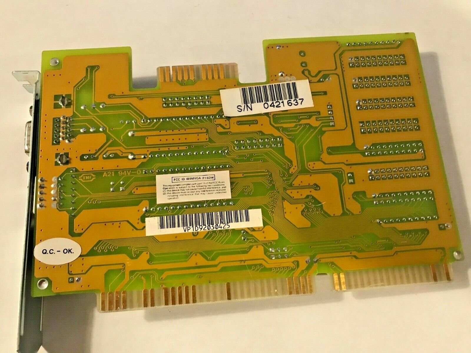
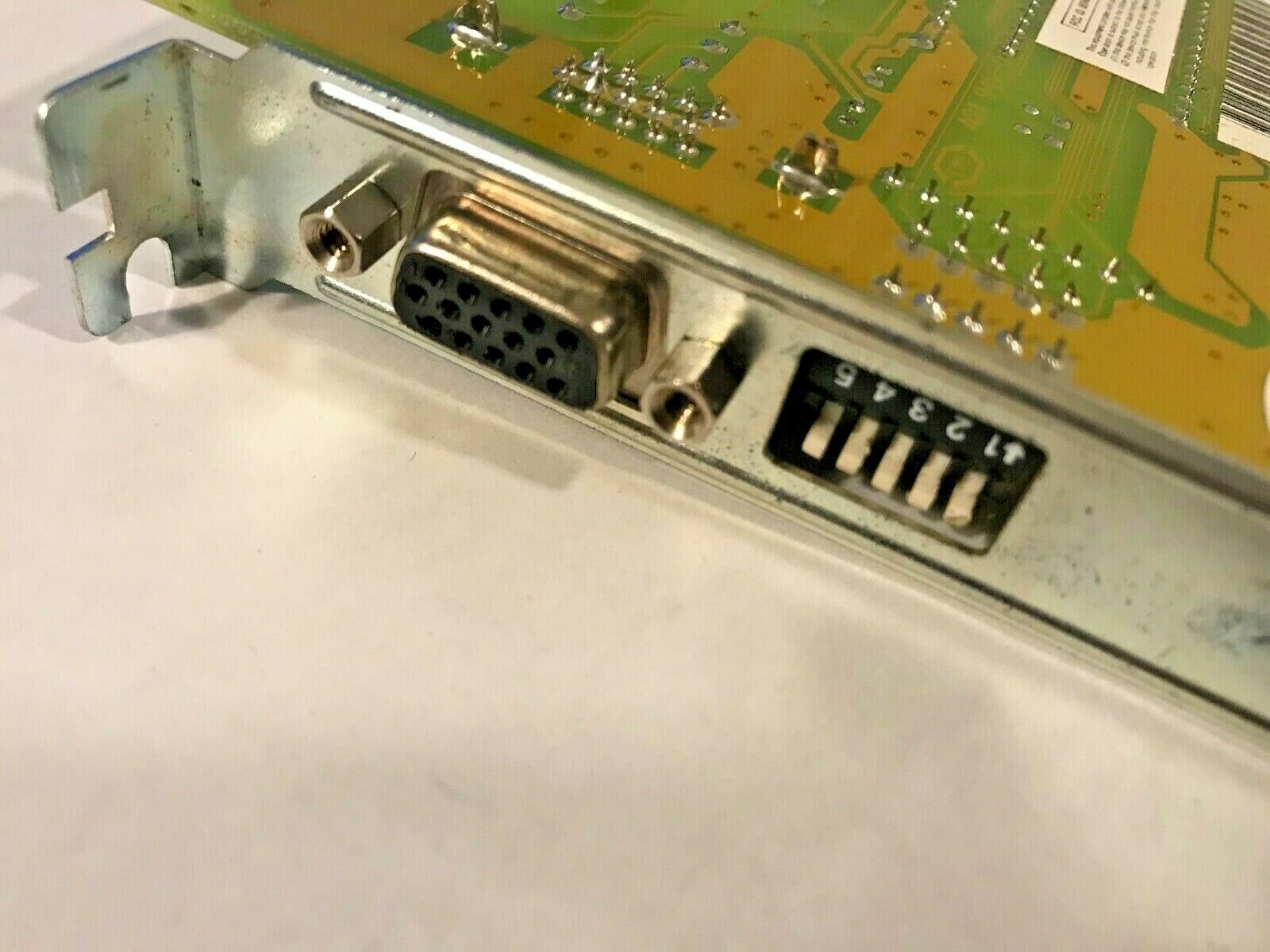
FCC ID: I7APVGAID, IB9MVGA P16DW (ProLink)
BIOS Dates:
Known BIOS Versions:
A Super VGA card that uses the Western Digital WD90C30-LR chipset. Highlights of the WD90C30 chipset are:
- Resolutions up to 1024 x 768 in 256 colours (also 640 x 400, 640 x 480, 800 x 600, all in 256 colours)
- 132-column text mode and 6-16 pixels wide fonts
- Integrated CRT controller, sequencer, graphics controller and attribute controller
- Write buffer for zero wait state CPU write performance
- 8- or 16-bit data bus for I/O and memory. True 16-bit CPU-to-video memory transfer for all modes
- 16-bit or 32-bit memory interface with fast page operations
- Up to 80 MHz maximum video clock rate
- Up to 50 MHz maximum memory clock rate
- Supports all VGA modes if using two 64Kx16 DRAMs
- Full VGA hardware and BIOS compatibility
- EGA register-level compatibility on analog, TTL, and multi-frequency monitors
- Backward compatibility with MDA, CGA, EGA, Hercules and AT&T 6300.
- Flexible RAM options, including two, four or eight 64Kx16 DRAMs, or four or eight 256Kx4 DRAMs, or one or two 256Kx16 DRAMs.
The VESA BIOS extensions in the VGA ROM BIOS are version 1.01. With the UNIVBE equivalent this can be extended to offer more modes:
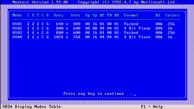
Built-in VESA modes (left) and with UNIVBE 6.70 installed (right)
I have done some benchmark testing with a Northman Technologies card with this chipset, in my 4-part C&T 386 Revival article, and also in my OPTi 386/486 Hybrid motherboard review (page 2). The WD90C30 is a very high-performing ISA-based SVGA chip, with ...
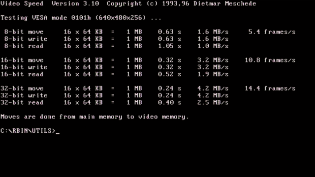
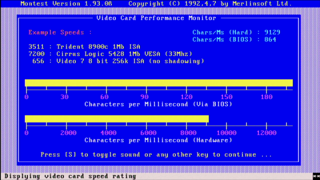
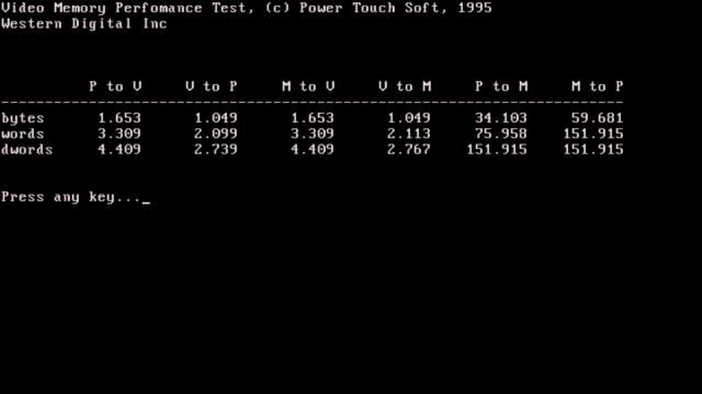
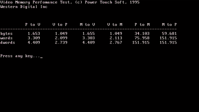
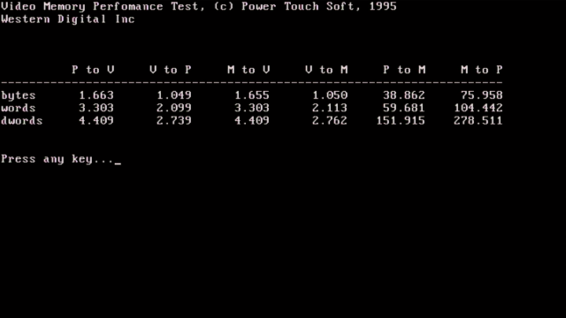
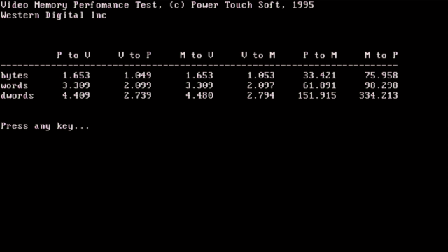

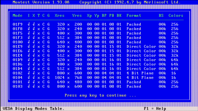
Top: Vidspeed (left) and MonTest (right)
Bottom: VInfo in 320x200, 640x400, 640x480, 800x600 and 1024x768 modes, all in 256 colours
The above performance tests were conducted on a Northman Technologies WD90C30-LR with 512 KB of Fujitsu-branded (61C4256A) 70ns video RAM. The host PC was a Pentium MMX 233 on a Gigabyte GA-5AX motherboard with 32 MB of RAM.
Video BIOS ROM shadowing was enabled in the BIOS.
VInfo tests a video card's memory performance, copying data between processor (P), video memory (V) and main memory (M), using three different-sized blocks and reports the data transfer rate in MB/sec.
Aimed at the high-end desktop market, the WD90C30 is a VGA controller chip for PC, XT, AT, and PS/2 systems and is implemented either directly on the motherboard or as an enhancement board.
The WD90C30 provides software driver support for Microsoft Windows, OS/2, Presentation Manager, AutoCAD, and Lotus 1-2-3, and support for VESA standard refresh rates of up to 1,024-by-768 noninterlaced resolution with 256 colors.
Other features include zero-wait-state performance; enhanced memory configuration for three types of DRAM (64K by 16, 256K by 4, and 256K by 16); and XGA capability with 65,536 simultaneous colors at 640-by-480 resolution for the support of multimedia applications.
Samples in 132-pin packages are now shipping and are priced at $30 in quantities of 1,000. Production quantities will be available in July.
The company is also working with Microsoft to ensure that its drivers will be part of Microsoft's multimedia extensions to Windows."
InfoWorld, 8 April 1991
Cards that use this include:
- Northman Technologies WD90C30-LR (512 KB) (FCC ID: I7APVGAID)
- Octek PVGA1D (V4201D) (512 KB or 1 MB)
- ProLink Microsystems MVGA (1 MB) - see 2nd, 3rd and 4th images below (FCC ID: IB9MVGA P16DW)
- Data Expert XP6678 (1 MB)
- Formosa Microsystems FM-V902Z (FCC ID: ILUFM-V902)
PCs that came bundled with the WD90C30-LR graphics card include:
- GRiD MFP/450 (486DX2-50 machine, 512 KB card)
- Softworks Development Citus MDC (486DX2-50 machine, 1 MB card)
- Dell System 486D/50 (embedded on motherboard, 1 MB video RAM)
In September 1992, Windows 3.1 drivers for the WD90C30-LR video chipset were still not available.
Click here for the WD90C30 datasheet.
More Images
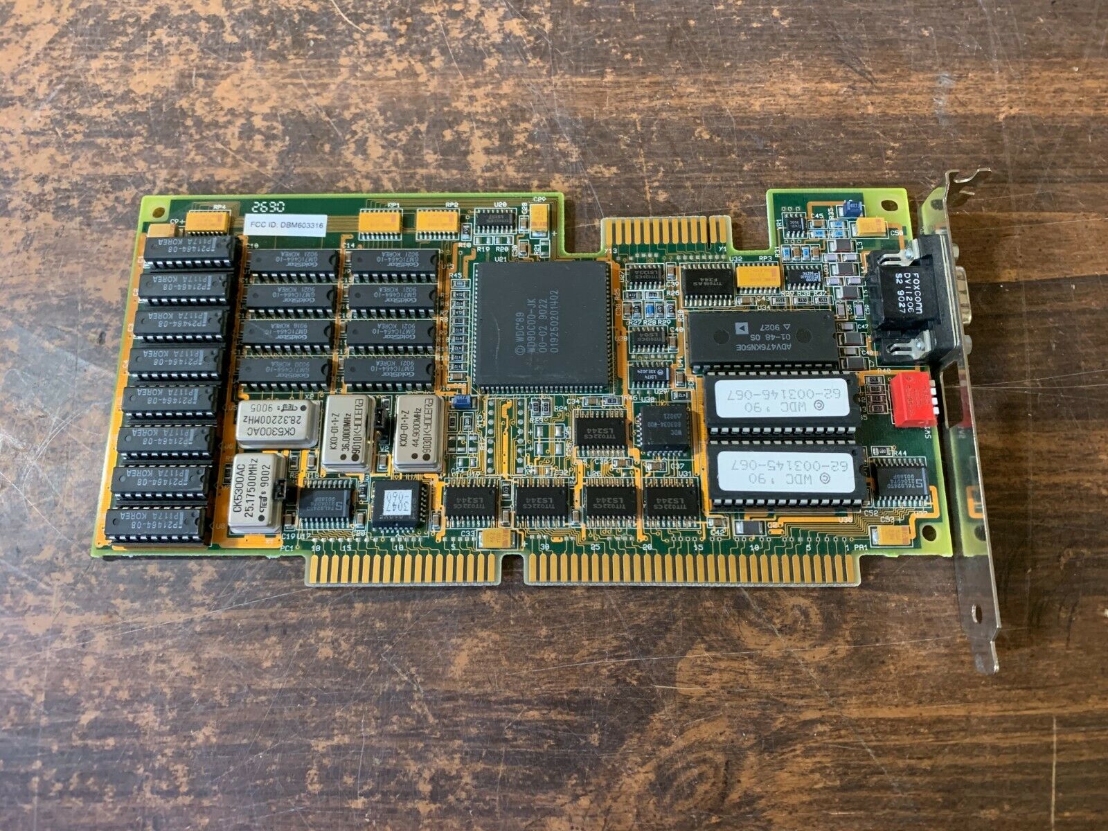
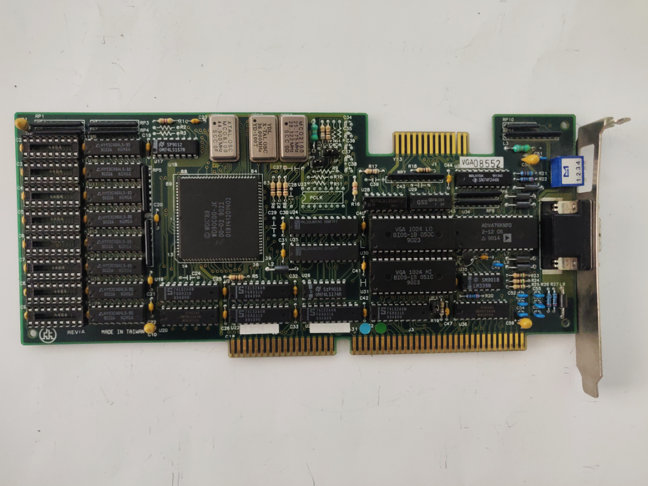
VGA 1024
Launched: 1991
Bus: ISA 16-bit
Memory: 512 KB
Price When New: $254 (Aug '91), $139 (Jun '92)
CONS: No 1MB version, no flicker-free modes, slow AutoCAD performance
Like the Genoa SuperVGA 6400A, the Paradise VGA 1024 tops out at 512K— and at $254 on the street, it sells for about the same price. It's the only board in the roundup that won't refresh the screen at 70 or 72 Hz in any mode.
The board is easy enough to install; there are no jumpers to set, just two DIP switches. However, switching drivers could be simpler—you have to do it from the DOS prompt instead of from a menu.
The board includes drivers for all the usual applications, but the memory cap means you won't find any 256-color drivers for 1024 by 768 operation—a disappointment if you're a business graphics user interested in previewing slides. Furthermore, compared with the other entries, this board performs slowly with AutoCAD.
For beyond-VGA graphics, the Paradise VGA 1024 falls short. You can do better for less." PC World, August 1991
WD90C22 
Launched: 1991
Bus: ISA 16-bit
Memory: 256 KB, 512 KB or 1 MB (FPM DRAMs)
RAMDAC Speed: 45 MHz (CRT) or 32 MHz (LCD)
The WD90C22 was a superset of the earlier WD90C00 chipset, primarily designed for use with LCD flat panel displays.
Click here for the WD90C22 datasheet.
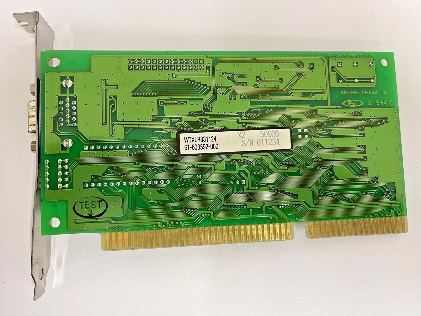
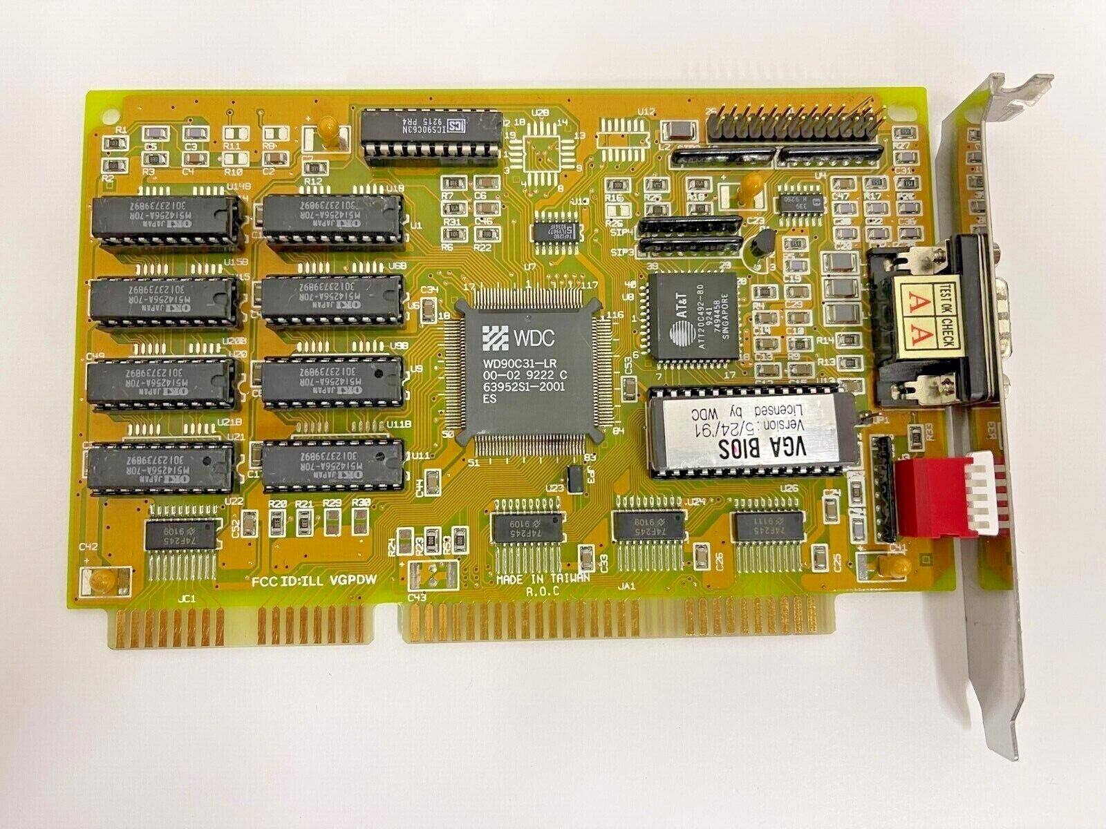
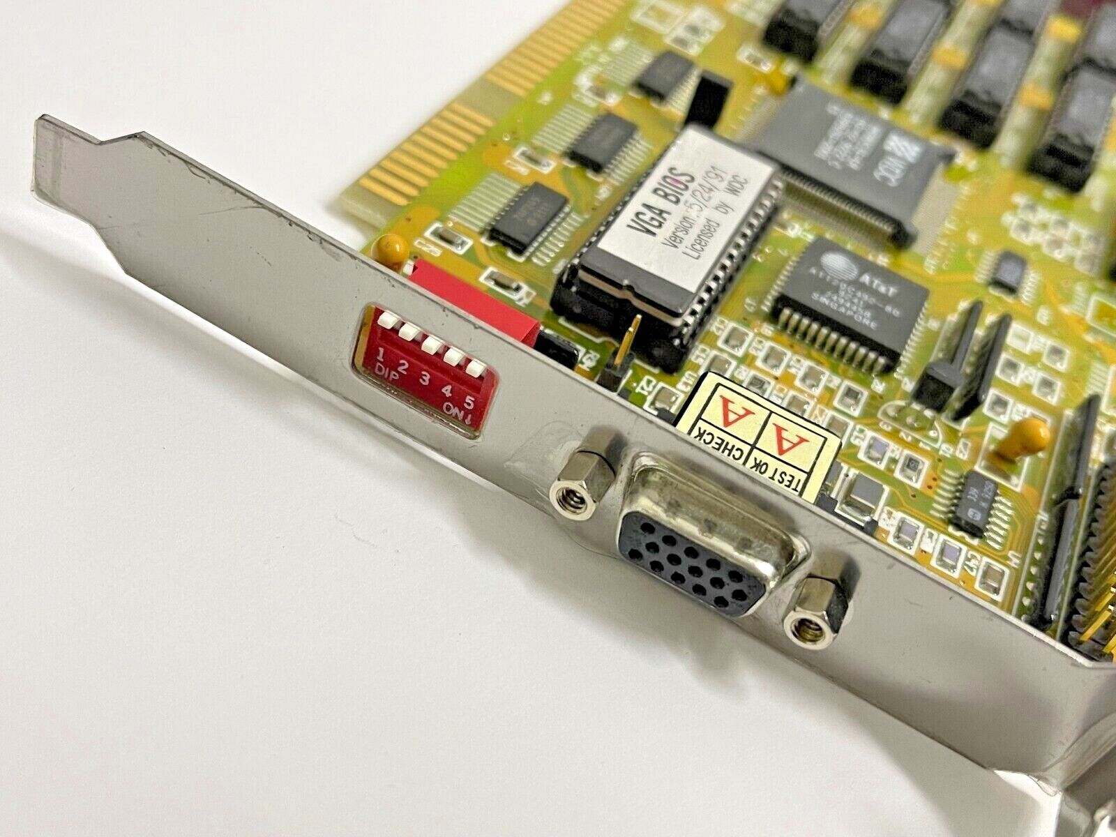
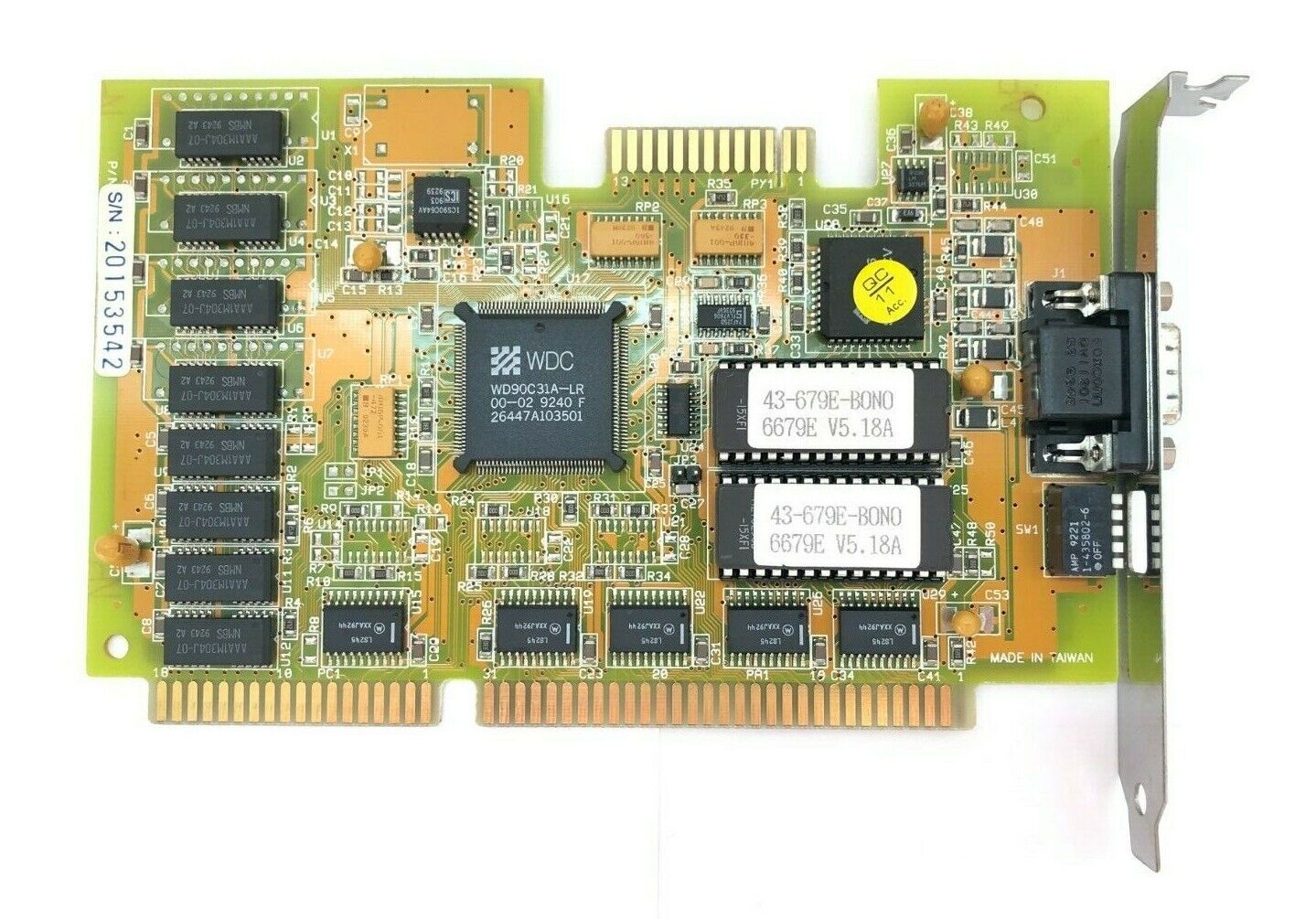
 WD90C31
Launched: 1992
Bus: ISA 16-bit
Memory: 1 MB
RAMDAC: Sierra Semiconductor SC15025CV
RAMDAC Speed: 80 MHz
VESA Standard: None
FCC ID: DBM603592 (Paradise Accelerator 24), ILLVGPDW (Britek 1 MB)
BIOS Dates:
Known BIOS Versions:
This, I believe, was the first card to be released after Philips acquired Western Digital Imaging (formerly Paradise Systems).
Probably the most prominent card to use the WD90C31 was the Diamond SpeedSTAR 24X. It uses a TrueColor DAC which provides 16.7 million colours.
I have no information on this chipset or the card shown above (and first two below), aside from the fact it is reportedly made by Philips. Pics 3 through 5 below are a Britek Electronics 1 MB card with FCC ID: ILL VGPDW.
This chip set has consistently generated balanced DOS-based and Windows graphics results during previous tests, and is a good general-purpose video chip set."
PC Magazine, September 1992
PCs that came bundled with the WD90C31 graphics card include:
- AST Power Premium 4/50d (486DX2-50 machine)
- Austin 486 WinStation DX2-50 (Paraise M6V card with 1 MB video memory)
Click here for the WD90C31 datasheet.
More Images
 WD90C33-ZZ
![]()
![]()
![]()
![]()
![]()
Launched: 1993
Bus: VESA Local Bus
Memory: 1 MB (expandable to 2 MB)
RAMDAC: ?
RAMDAC Speed: ?
VESA Standard: ?
FCC ID: DXL9ILC677 (Lung Hwa Electronics)
BIOS Dates: ?
Known BIOS Versions: ?
This card is capable of 1280 x 1024 (interlaced). The FCC ID can be mis-read as DXL9ILC077.
Click here for the WD90C33 datasheet
More Images
WD90C24 
Launched: 1994
Bus: ISA 16-bit and VESA Local Bus
Memory: 256 KB, 512 KB or 1 MB (FPM DRAMs)
RAMDAC Speed: 45 MHz (32 MHz for LCD)
The WD90C24 features hardware Windows 2D acceleration with BitBlt and line draw functions, and a programmable 64x64 cursor. WD90C24 has a 16- or 32-bit memory interface from 256 KB up to 1 MB (70, 80 or 100ns), and supports up to 65,536 colours (HiColor) at 640x480. The maximum resolution is 1024x768 in 256 colours noninterlaced at 60 Hz, or 1024x768x16 interlaced at 43 Hz.
Click here for the WD90C24 datasheet.
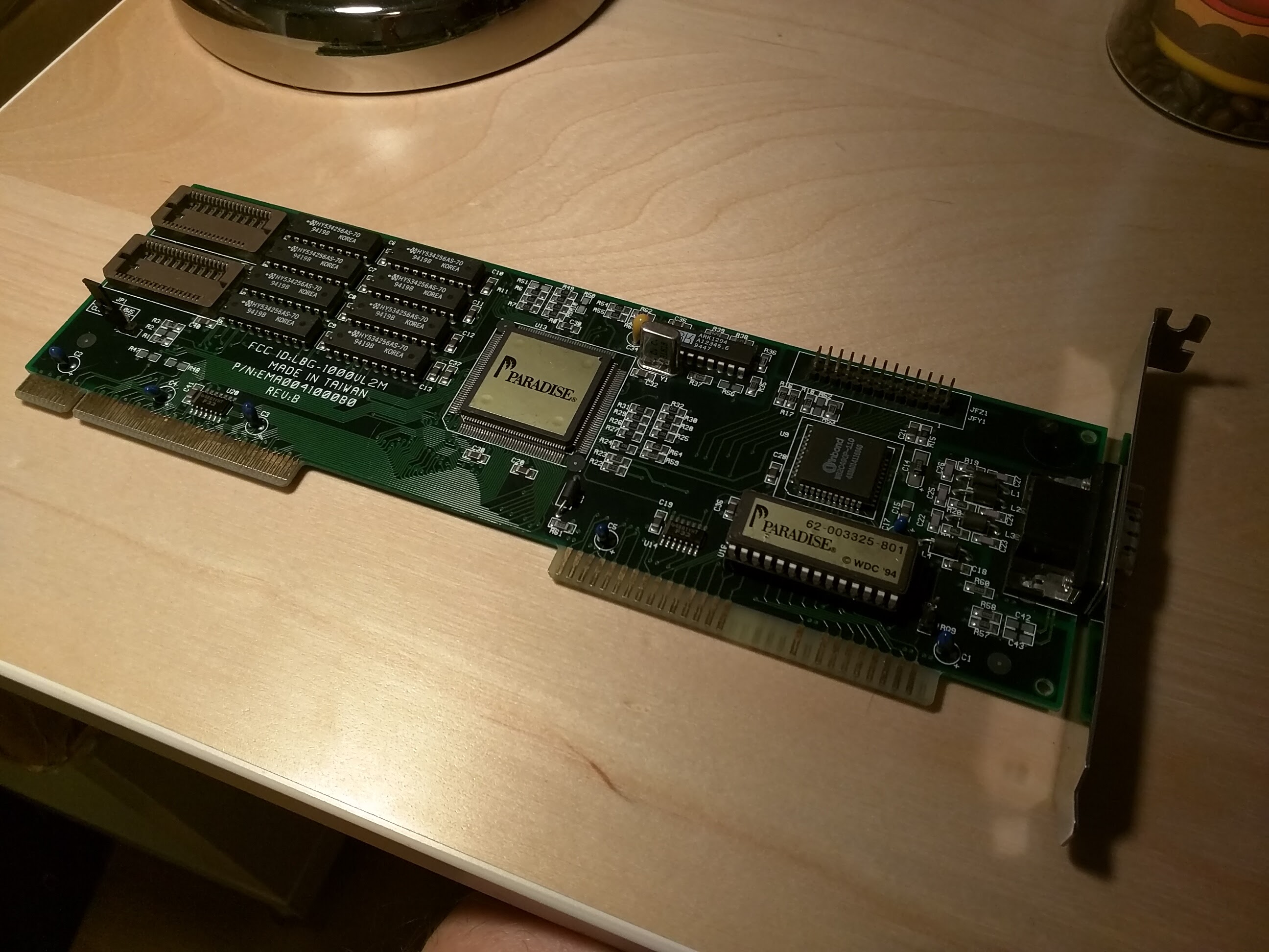 Unknown Paradise Card
Launched: 1994
Bus: VESA Local Bus
Memory: 1 or 2 MB?
RAMDAC: ?
RAMDAC Speed: ?
VESA Standard: ?
FCC ID: L8G-1000VL2M (Lantech Advance Corp.)
BIOS Dates: ?
Known BIOS Versions: ?
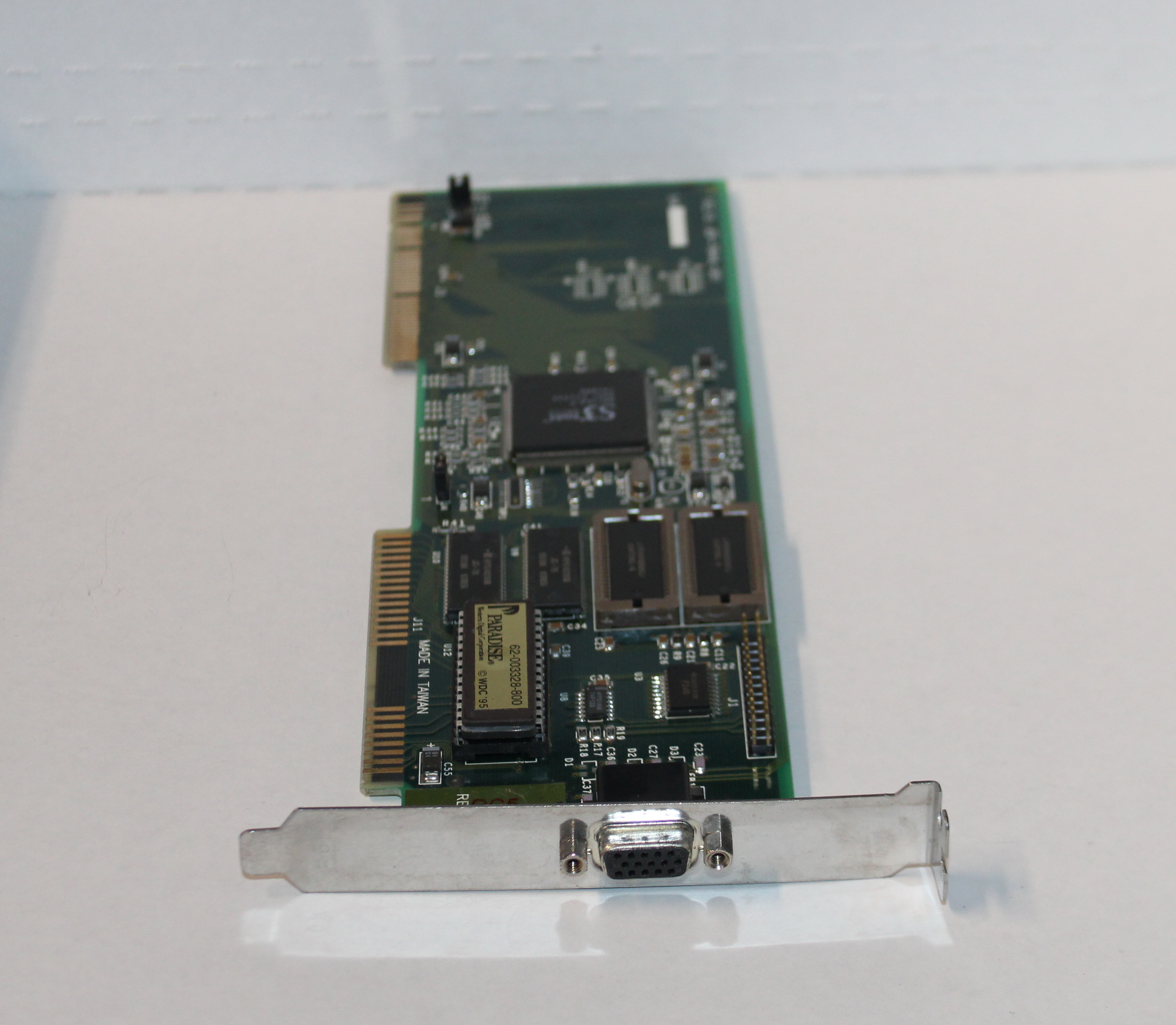
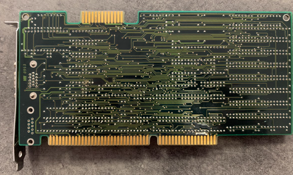
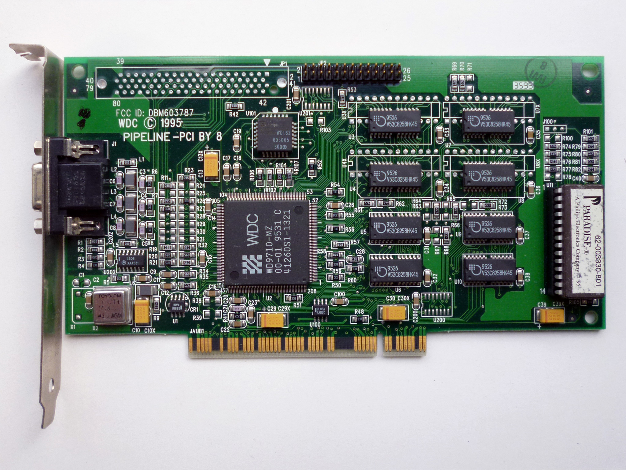 Pipeline PCI 8 / Pipeline 64 / Pipeline 64 HQ / Pipeline PCI BY 8
![]()
![]()
![]()
Launched: 1995
Bus: PCI
Chipset: Western Digital RocketChip WD9710-MZ
Memory: 1 or 2 MB EDO DRAM
RAMDAC: ?
RAMDAC Speed: ?
VESA Standard: Yes
Part #: WDC 60-603787-005
FCC ID: DBM603787
BIOS Dates: ?
Known Board Revisions: X5
Known BIOS Versions: ?
The WD9710-MZ was a full 64-bit graphics and motion video accelerator chipset released in March 1995. This high-performance chipset allowed for up to 320 MB/sec data throughput. The onboard RAMDAC supports 24-bit TrueColor (16.7 million colours) at resolutions up to 1024 x 768, with a maximum resolution of 1600 x 1200 at 256 colours. It also had hardware BitBlt operations for 8-, 16- and 24-bit colour modes. It supported PCI and VESA Local Bus interfaces.
The full motion aspects of the WD9710-MZ supported hardware MPEG-1 compression.
The memory is held in two banks each comprising of four SOP package EDO SDRAM memory ICs. Bank 0 is the lowest four chips and these are soldered in. Bank 1 is the upper four chips/sockets. Up to 4 MB of video memory is supported by the WD9710, though most graphics cards based around this chip came in 1 MB and 2 MB versions only.
Intended primarily for integration into PC motherboards, the RocketChip WD9710 chip will also be available in third-party boards, said Leonard Sharp, vice president of marketing for the company. Boards and systems based on the chip will ship in the second quarter of next year and are expected to cost about $299, he said.
The RocketChip WD9710, a 64-bit chip, will normally ship with 2MB of DRAM, allowing it to display noninterlaced resolutions as high as 1,280 by 1,024 with 256 colors.
The chip will also take motion video at a resolution of 320 x 240 and scale it up to 640 by 480 without any noticeable fuzziness and without dropping frame rates, Sharp said.
The chip is optimized to support MPEG1, Cinepak, Indeo, and any other codec (compression/decompression) that supports the Microsoft Corp. and Intel Corp. Display Control Interface driver specification, the company said.
Boards based on the chip will accelerate any application under Windows, Windows 95, OS/2, SCO Unix, and AutoCAD, and MicroStation under DOS. In addition, the chip supports Microsoft's Plug and Play specification and VESA's Display Data Channel 1 and 2 monitor specification.
The chip supports the PCI bus, among others, and will work in Mac or PC boards, said Western Digital. The company plans to develop a version of the chip for portables later in 1995, Sharp said."
InfoWorld, 3 Oct 1994
The provided CD-ROM included Windows 95 drivers, a video player and "Oasis95" Windows configuration software.
Click here for the WD9710 datasheet.
The WD9710 chip competed directly with the following chipsets/cards:
- ATi Mach64
- Matrox MGA-2064W (example card: Matrox Millennium)
- S3 Vision 968 (example cards: Number Nine FX Motion771, $599, and STB Systems Velocity 64V, $449)
- VideoLogic PowerPlay 64
- I.C. Works ZoomDAC (example card: Hercules Stingray 64, $250)
- Weitek Video Power (example card: Diamond Viper Pro Video, $649)
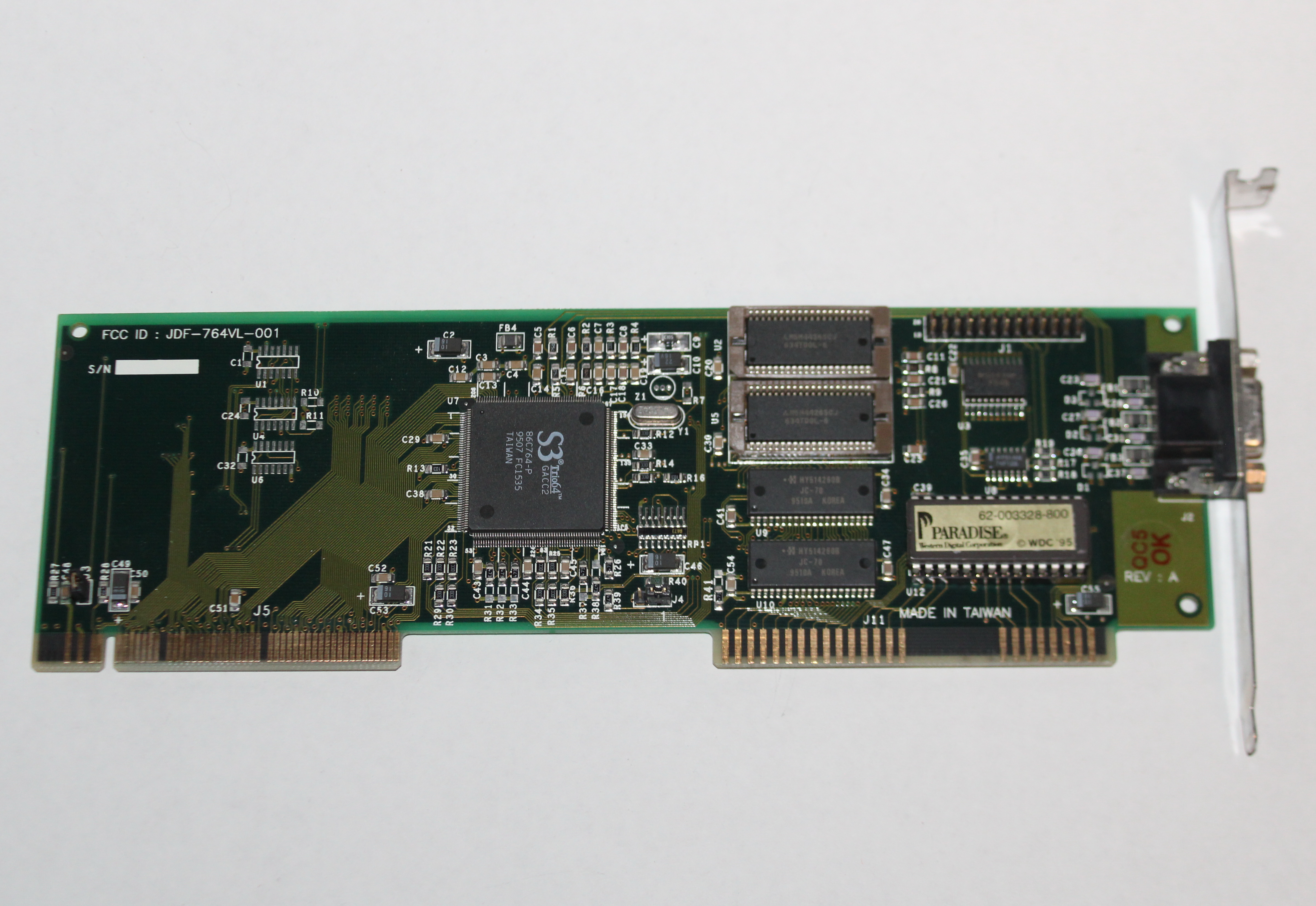
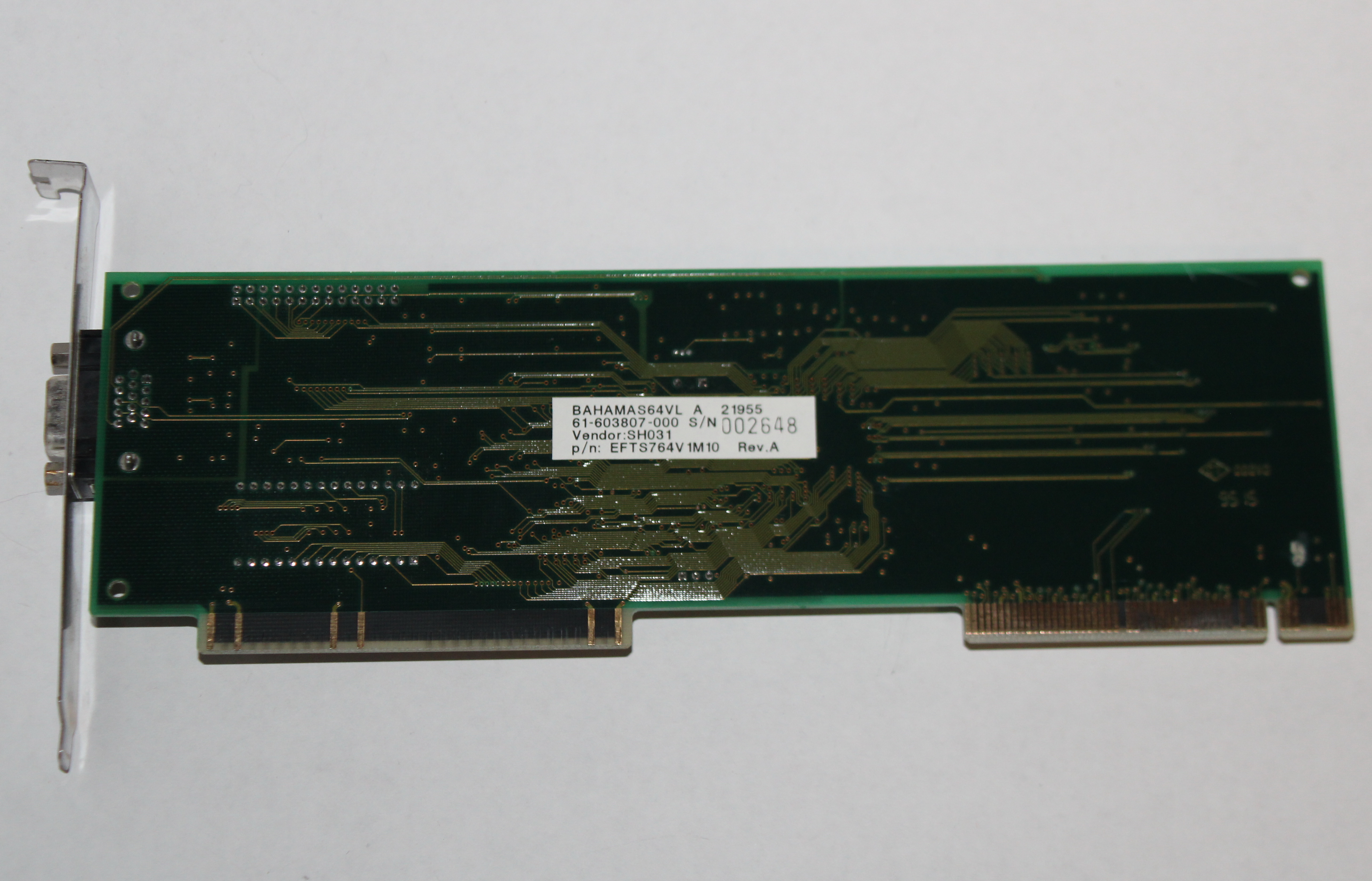
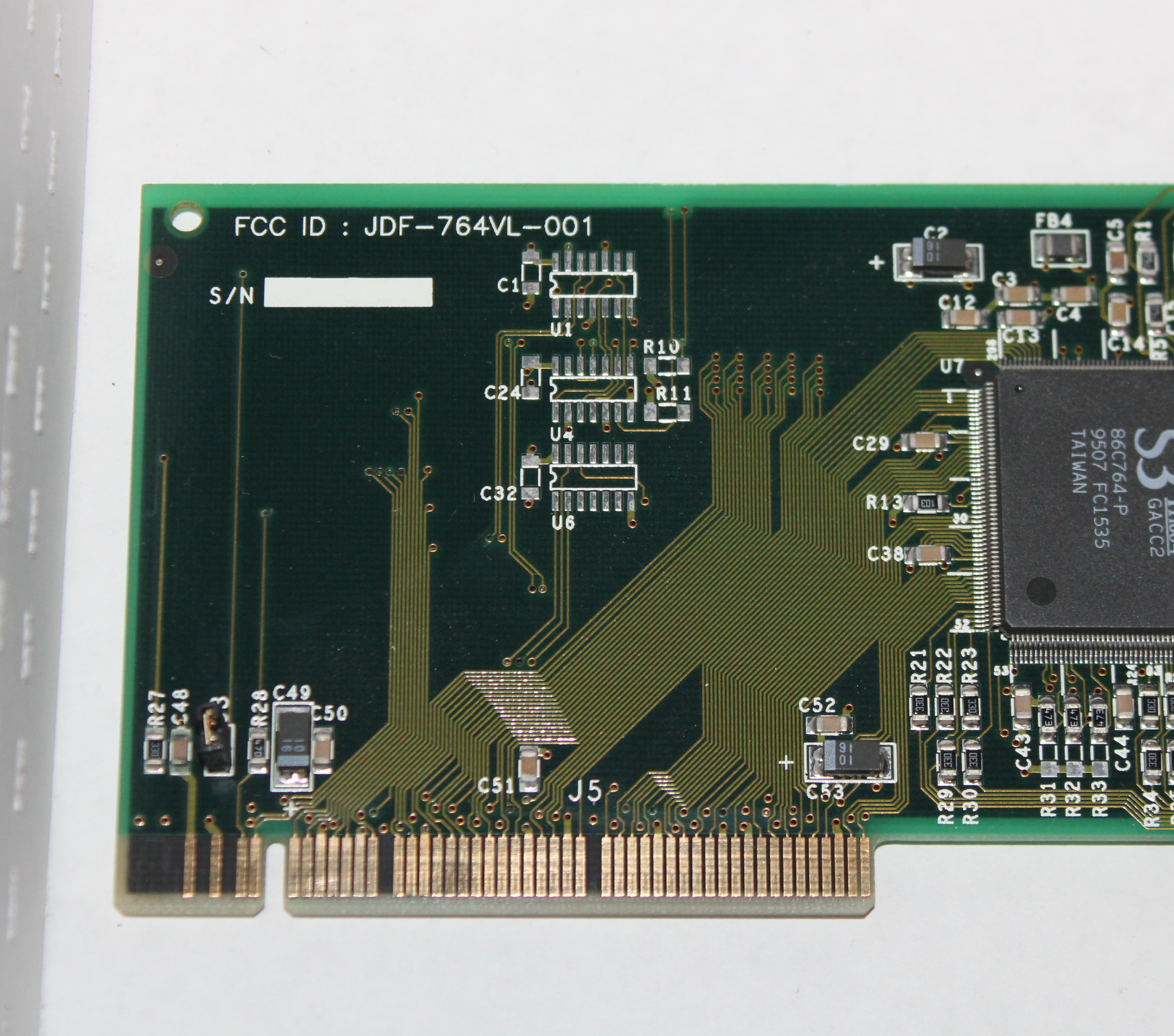
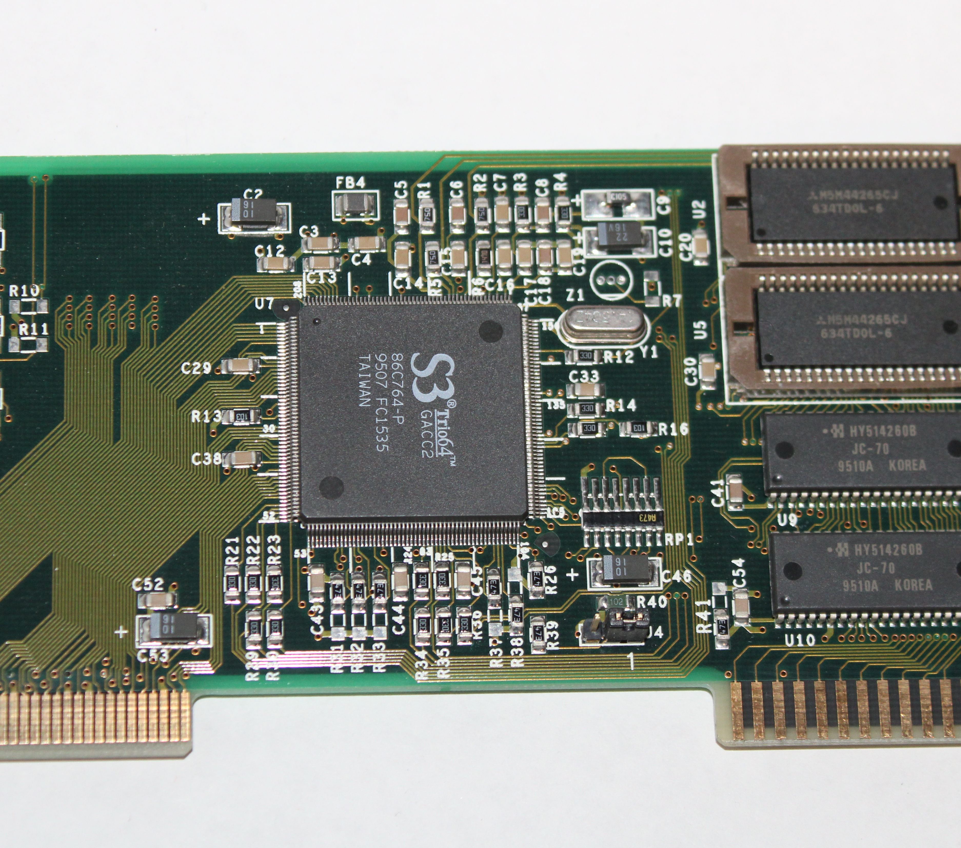
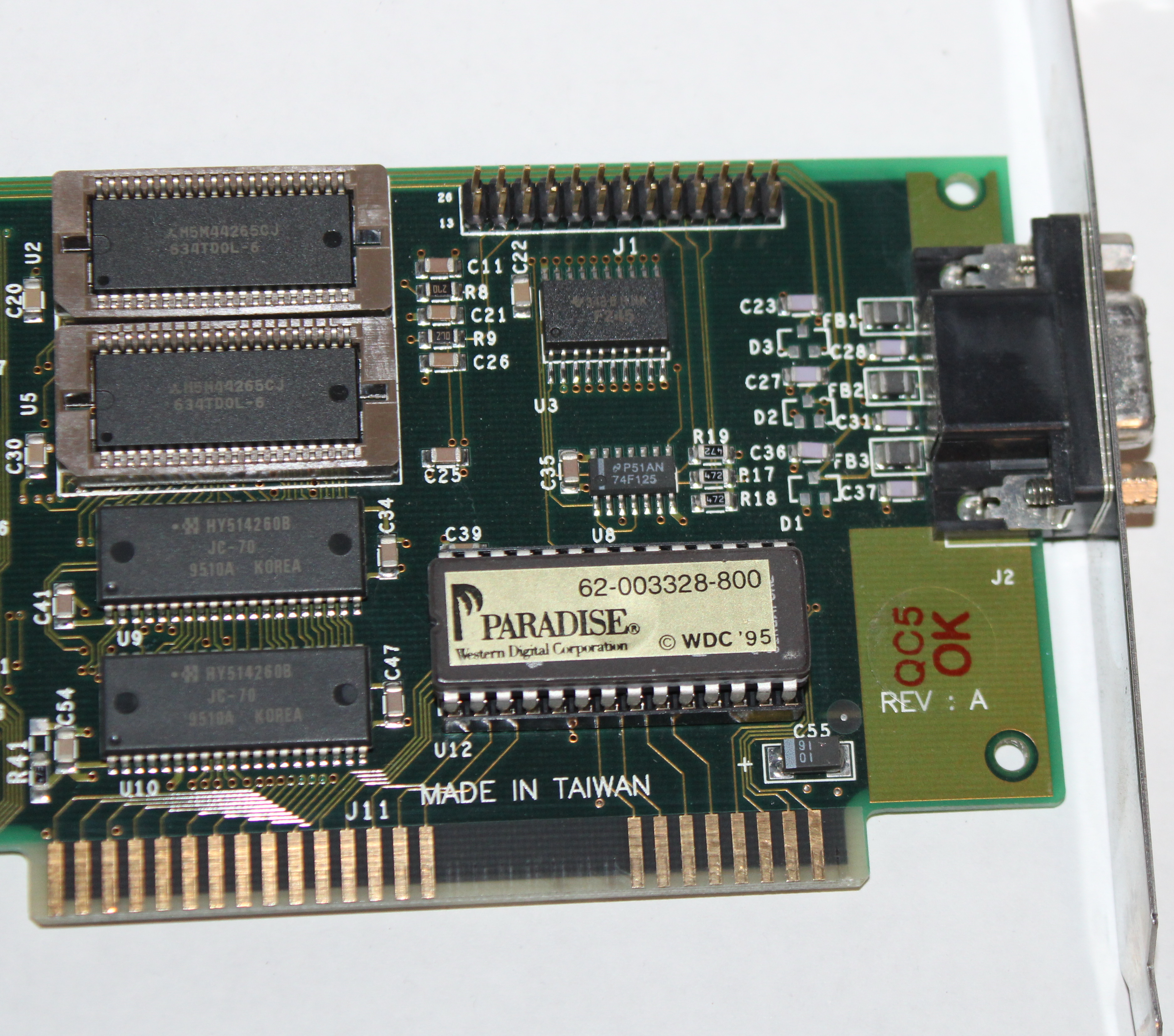
.png) Bahamas 64VL
Bahamas 64VL
![]()
![]()
![]()
Launched: 1995
Bus: VESA Local Bus
Chipset: S3 Trio64 (86C764)
Memory: 1 or 2 MB DRAM
RAMDAC: (Integrated)
RAMDAC Speed: 135 MHz
FCC ID: JDF-764VL-001
Cost When New: $199
The Bahamas64VL was a 64-bit DRAM-based accelerator card for Windows. Based around the S3 Trio64 graphics chipset, it featured hardware cursor, BitBLT, pattern fills, short stroke vector and line draws in hardware. A PCI-based version was also released called the Bahamas 64.
The Bahamas64 sat in the middle of their 1995 trio of graphics accelerator cards. At the lower end was the cheaper Bali 32 graphics card (also available in VLB and PCI) had just 1 MB of DRAM video memory (upgradable to 2 MB) and retailed for $99. Meanwhile at the top end was the Barbados 64, which was only available in PCI form, but came with 2 MB of VRAM and retailed for $299.
All images shown for this card are courtesy of Andrew Welburn from Andy's Arcade.
More Images
Paradise/Western Digital Crystals
Most Paradise and Western Digital SVGA graphics cards come with 3 or 4 crystal oscillators, which are defined as follows:
MCLK is the memory clock and determines the DRAM read/write access timing as well as the system CPU I/O and memory timing. MCLK should be 36 MHz if 120ns DRAMs are installed, and 42 MHz if 100ns or faster DRAMs are installed. This crystal should be of a higher value than VCLK0 and VCLK1.
VCLK0 is the video display clock (aka, the dot clock) for both text and graphics modes. At 25.175 MHz, this displays 640 pixels per horizontal display line.
VCLK1 can either be a second video display clock input or an output to an external clock selection module. If used as an input, 28.322 MHz is used to display 720 pixels per horizontal display line.
VCLK2 (if a fourth crystal is present) can either be a third video display clock input, or an output to an external clock selection module. If present it is usually 42.000 MHz or 44.900 MHz - don't confuse VCLK2 with MCLK. If the card also has a 36 MHz crystal elsewhere, that one is likely to be your MCLK crystal, and the 42 or 44.9 MHz one would be VCLK2. Your card might have a jumper to enable this fourth crystal, i.e. VCLK2.
For 320 or 360 pixel modes, VCLK0, VCLK1 or VCLK2 is divided by 2 by the chipset to derive the pixel clock (PCLK).